
Photovoltaic cell comprising a thin lamina having emitter formed at light-facing and back surfaces

a photovoltaic cell and emitter technology, applied in the field of photovoltaic cells comprising thin laminas, can solve the problems of reducing the likelihood of recombination before reaching the collecting junction, and forming a heavily doped emitter region at both the light-facing and back surfaces of a photovoltaic cell,

Inactive Publication Date: 2011-03-31
GTAT CORPORATION
View PDF7 Cites 29 Cited by
  • Summary
  • Abstract
  • Description
  • Claims
  • Application Information

AI Technical Summary

Benefits of technology

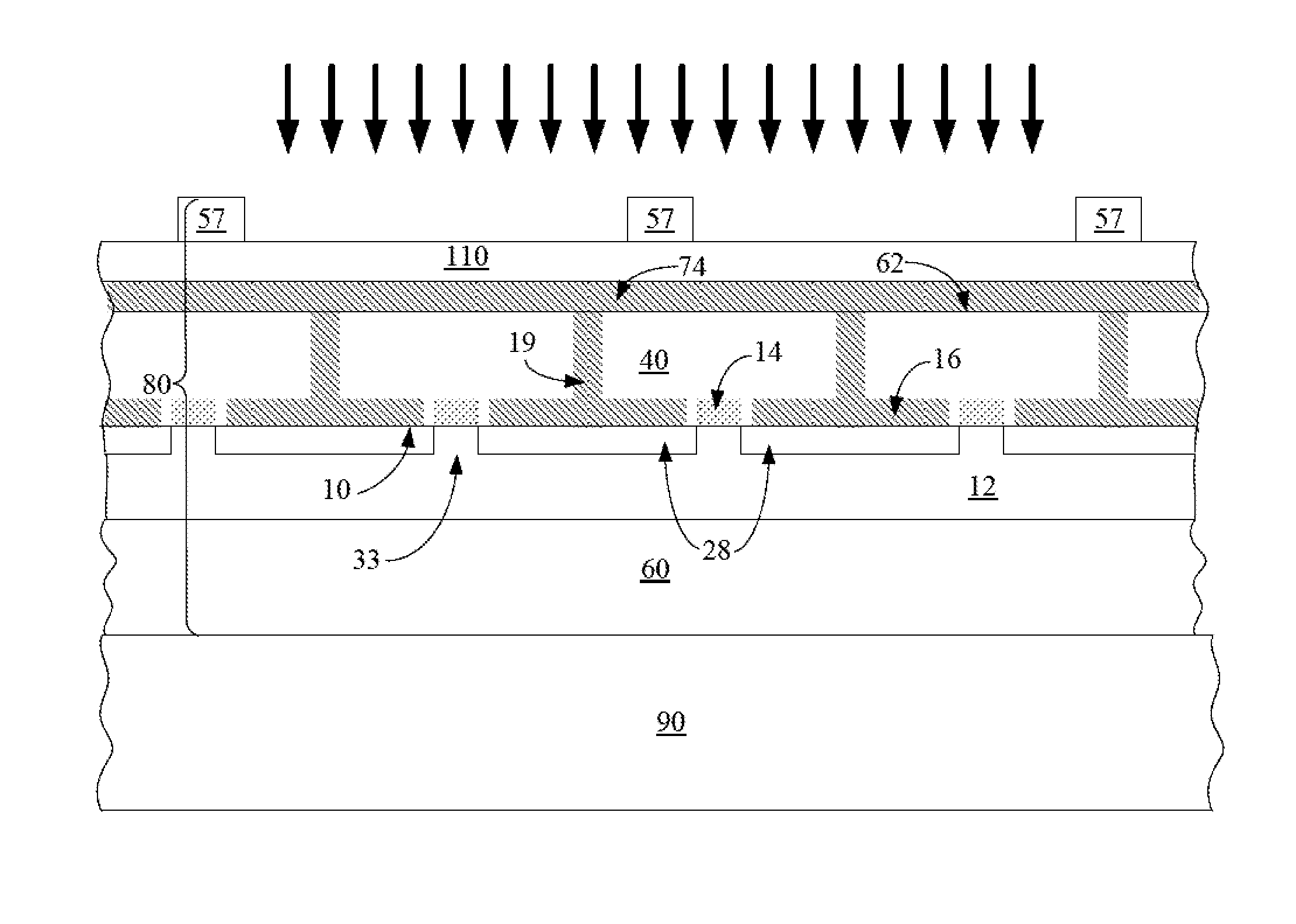
[0007]Another aspect of the invention provides for a method to fabricate a photovoltaic cell, the method comprising the steps of providing a substantially crystalline semiconductor lamina having a light-facing surface and a back surface; and forming an emitter of the photovoltaic cell, wherein a fir

Problems solved by technology

Having emitter regions formed at both the light-facing surface and back surface of the cell decreases travel distance required for minority carriers, also decreasing the likelihood of recombination before reaching the collecting junction.
Forming a heavily doped emitter region at both the light-facing and back surfaces of a photovoltaic cell may be difficult when certain fabrication techniques are used to form the cell, however.

Method used


Image

  • Photovoltaic cell comprising a thin lamina having emitter formed at light-facing and back surfaces
  • Photovoltaic cell comprising a thin lamina having emitter formed at light-facing and back surfaces
  • Photovoltaic cell comprising a thin lamina having emitter formed at light-facing and back surfaces

Examples


example

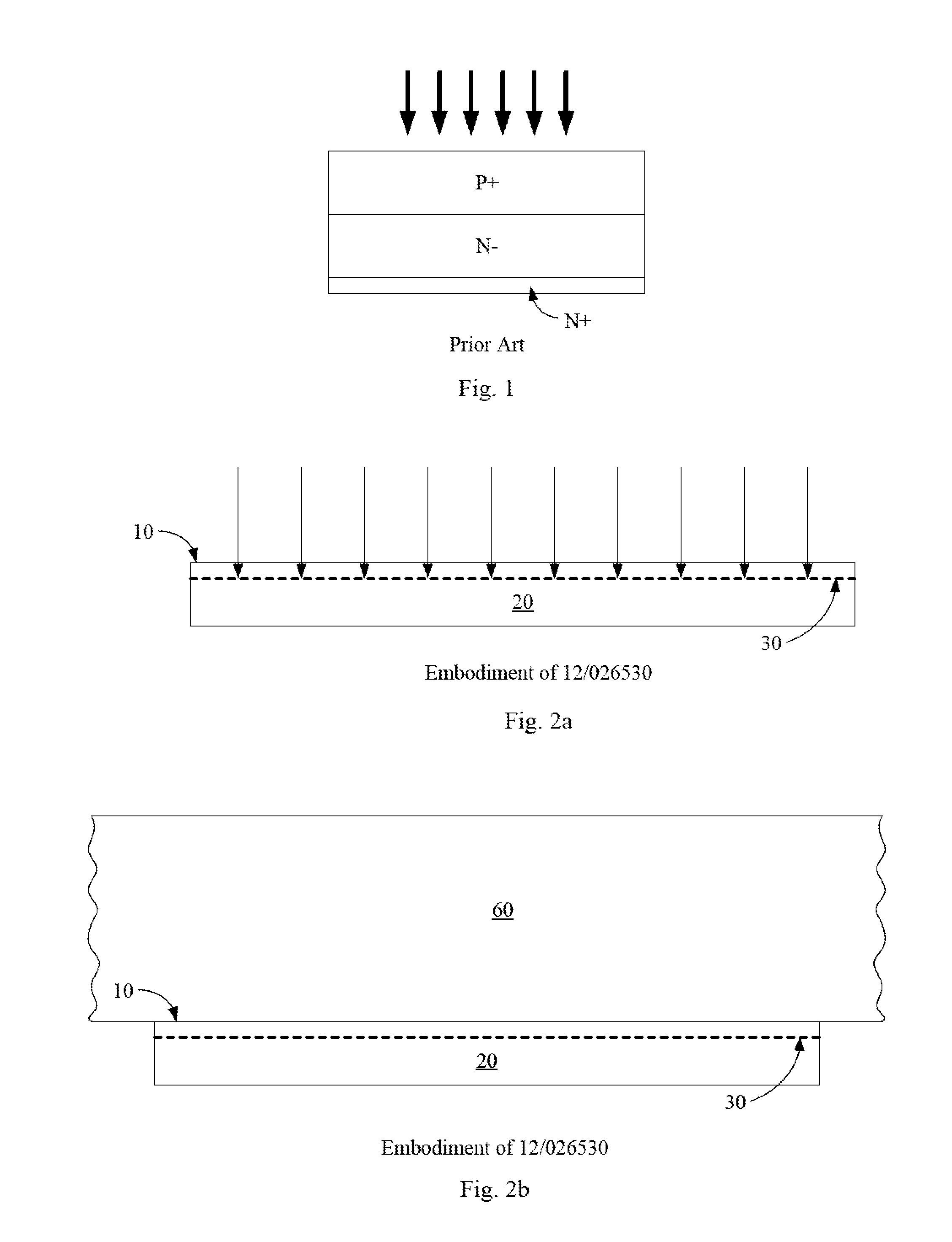
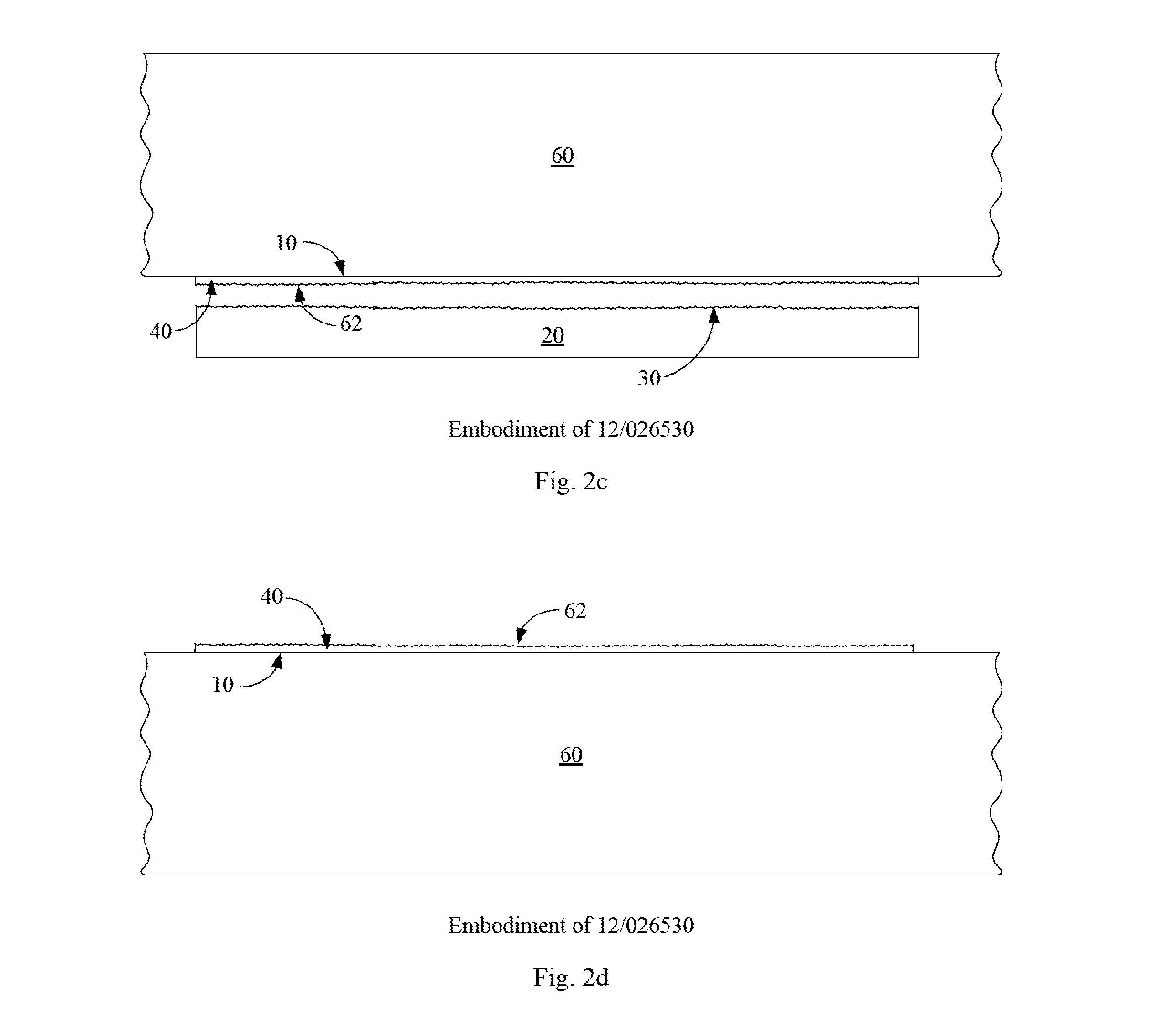
[0027]The process begins with a donor body of an appropriate semiconductor material. An appropriate donor body may be a monocrystalline silicon wafer of any practical thickness, for example from about 200 to about 1000 microns thick. In alternative embodiments, the donor wafer may be thicker; maximum thickness is limited only by practicalities of wafer handling. Alternatively, polycrystalline or multicrystalline silicon may be used, as may microcrystalline silicon, or wafers or ingots of other semiconductor materials, including germanium, silicon germanium, or III-V or II-VI semiconductor compounds such as GaAs, InP, etc., may be used. In this context the term multicrystalline typically refers to semiconductor material having grains that are on the order of a millimeter or larger in size, while polycrystalline semiconductor material has smaller grains, on the order of a thousand angstroms. The grains of microcrystalline semiconductor material are very small, for example 100 angstrom...


PUM


Abstract

A photovoltaic cell is described having emitter portions formed at both a light-facing surface and a back surface of the cell. In some embodiments, heavily doped emitter regions extend between the front and back emitter regions, connecting them electrically. Use of this structure is particularly well-adapted to a cell formed by implanting a semiconductor donor body with hydrogen and / or helium ions, affixing the donor body to a receiver element, cleaving a lamina from the donor body, and completing fabrication of a photovoltaic cell comprising the lamina. The emitter portion formed at the unbonded surface may comprise amorphous silicon. The lamina may be thin, for example 10 microns thick or less.

Description

BACKGROUND OF THE INVENTION[0001]The invention relates to a photovoltaic cell comprising a thin lamina, the photovoltaic cell having emitter regions at both its light-facing surface and its back surface.[0002]Minority charge carriers generated in the base of a photovoltaic cell must reach the emitter of the cell without falling into the valence band of an atom, or recombining, in order to contribute to the cell's photocurrent. Having emitter regions formed at both the light-facing surface and back surface of the cell decreases travel distance required for minority carriers, also decreasing the likelihood of recombination before reaching the collecting junction. Forming a heavily doped emitter region at both the light-facing and back surfaces of a photovoltaic cell may be difficult when certain fabrication techniques are used to form the cell, however.[0003]There is a need, therefore, for a method to form a photovoltaic cell having emitter regions at both light-facing and back surfac...

Claims


Application Information

Patent Timeline
IPC IPC(8): H01L31/00H01L31/18
CPCH01L31/022441H01L31/0682H01L31/03529H01L31/1896Y02E10/547H01L31/1804Y02P70/50
Inventor HILALI, MOHAMED M.PETTI, CHRISTOPHER J.
Owner GTAT CORPORATION
Learn More