Light-emitting device and display

Inactive Publication Date: 2011-03-31
SONY CORP
View PDF14 Cites 9 Cited by
  • Summary
  • Abstract
  • Description
  • Claims
  • Application Information

AI Technical Summary

Benefits of technology

[0006]In an organic EL element of this kind, light generated in the light-emitting layer is typically non-polarized light unless a material of the light-emitting layer has anisotropy. Therefore, most of the light generated in the light-emitting layer is absorbed by a pol

Problems solved by technology

However, in such a case, the number of components is in

Method used


Image

  • Light-emitting device and display
  • Light-emitting device and display
  • Light-emitting device and display

Examples


first embodiment

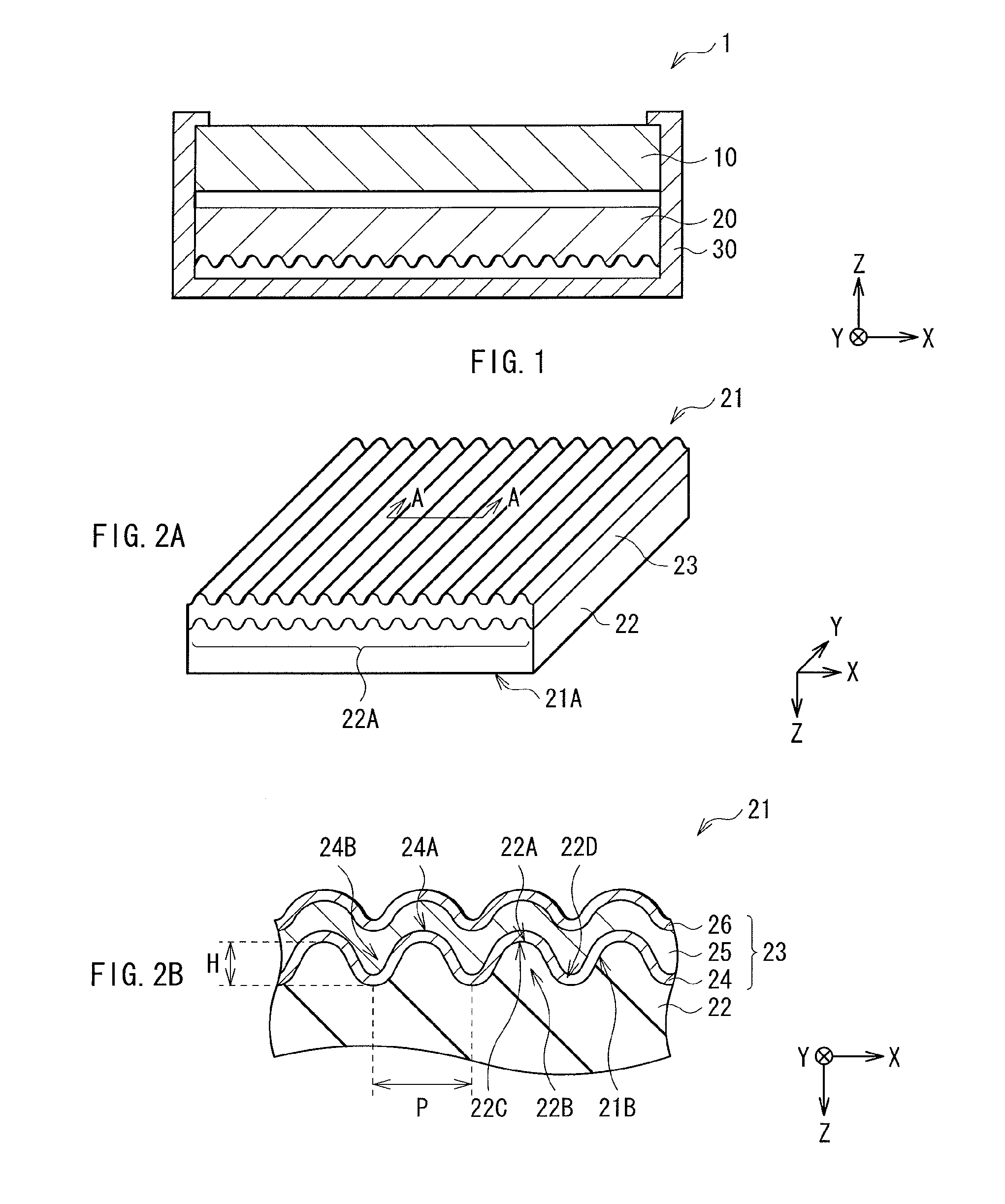
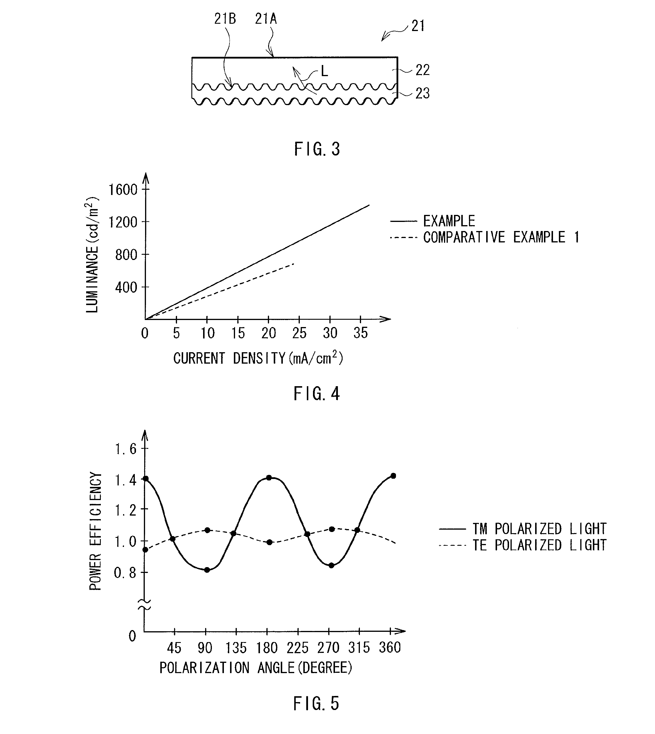
[0025]FIG. 1 illustrates an example of a schematic configuration of a display 1 according to a first embodiment. The display 1 includes a liquid crystal display panel 10 (a display panel), an illuminating device 20 arranged on a back surface of the liquid crystal display panel 10, an enclosure 30 supporting the liquid crystal display panel 10 and the illuminating device 20, and a drive circuit (not illustrated) driving the liquid crystal display panel 10 to display a picture. In the display 1, a front surface of the liquid crystal display panel 10 is oriented toward a viewer (not illustrated).

[0026]Liquid crystal display panel 10

[0027]The liquid crystal display panel 10 displays a picture. The liquid crystal display panel 10 is, for example, a transmissive display panel in which each pixel is driven in response to a picture signal, and has a configuration in which a liquid crystal layer is sandwiched between a pair of transparent substrates. The liquid crystal display panel 10 inclu...

second embodiment

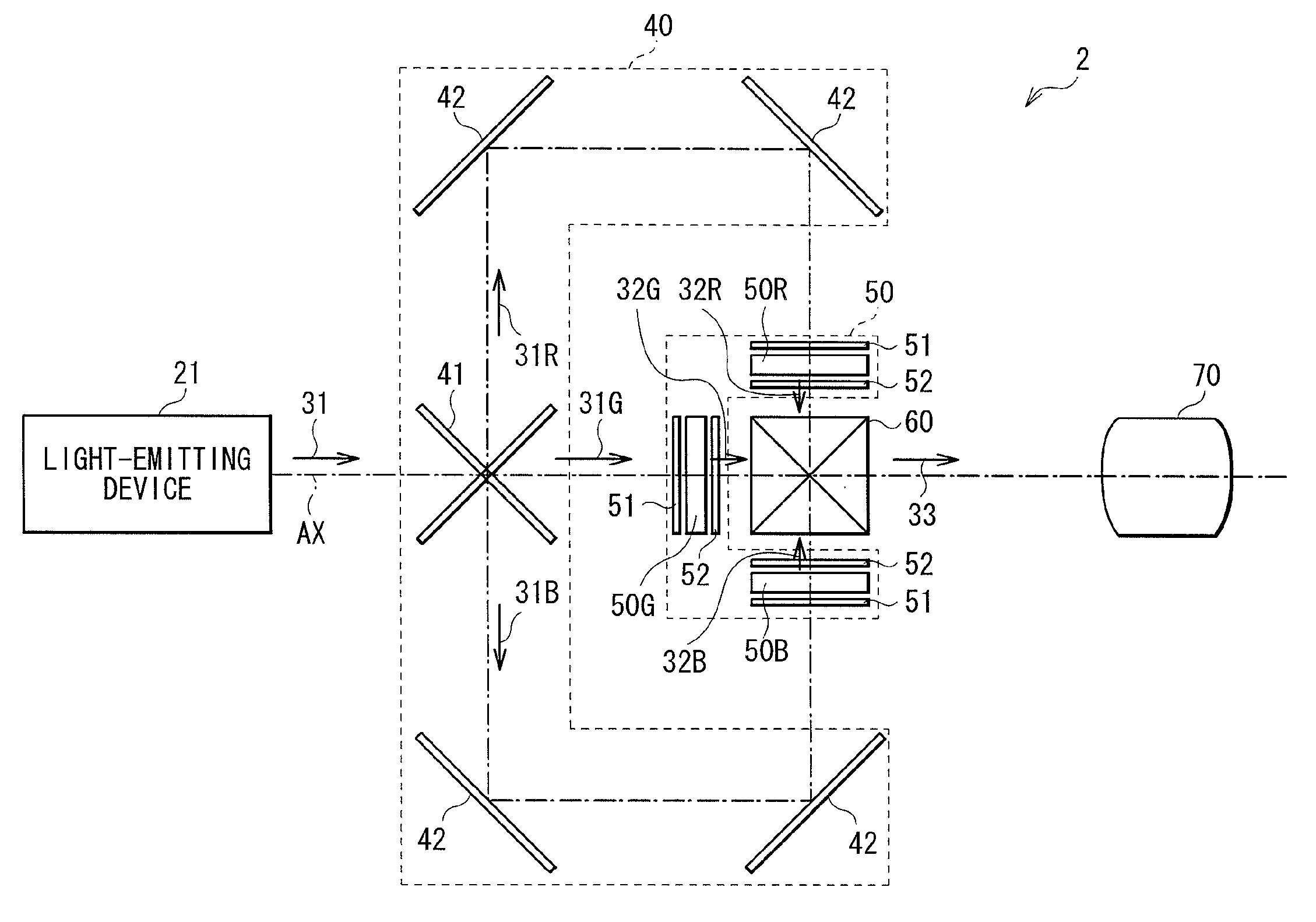
[0054]Next, a projector 2 according to a second embodiment will be described below. FIG. 8 illustrates an example of a schematic configuration of the projector 2 according to the embodiment. The projector 2 includes the light-emitting device 21 in the above-described embodiment as a light source of the projector 2.

[0055]The projector 2 is, for example, a three-panel transmissive LCD-projector, and as illustrated in FIG. 8, the projector 2 includes, for example, the light-emitting device 21, an optical path branch section 40, a spatial light modulation section 50, a synthesizing section 60 and a projection section 70.

[0056]The light-emitting device 21 supplies a luminous flux applied to an irradiated surface of the spatial light modulation section 50. In addition, if necessary, an optical element of some kind may be arranged in a region (on an optical axis AX) where light 31 from the light-emitting device 21 passes. For example, on the optical axis AX, an ND filter except for visible...


PUM


Abstract

A light-emitting device allowed to obtain polarized light without increasing the number of components or the thickness thereof, and a display including the light-emitting device are provided. The light-emitting device includes: a light-emitting element including, on a substrate, a first electrode, a light-emitting layer and a second electrode in order from the substrate. The substrate has, on a surface facing the first electrode, a first concavo-convex structure including a plurality of strip-shaped protrusion sections with a width equal to or smaller than an upper wavelength limit of visible light, and the first electrode, the light-emitting layer and the second electrode each have, on a surface opposite to a surface facing the substrate, a second concavo-convex structure imitating the protrusion sections of the first concavo-convex structure.

Description

CROSS REFERENCES TO RELATED APPLICATIONS[0001]The present application claims priority to Japanese Priority Patent Application JP 2009-224899 filed in the Japan Patent Office on Sep. 29, 2009, the entire content of which is hereby incorporated by reference.BACKGROUND[0002]The present application relates to a light-emitting device including a light-emitting element such as an organic electroluminescence element (an organic EL element), and a display including the light-emitting device.[0003]Cold cathode fluorescent lamps have been heretofore used widely as backlights of liquid crystal displays. The cold cathode fluorescent lamps have superior characteristics including an emission wavelength range, luminance and the like, but a reflective plate, a light guide plate or the like is necessary to irradiate a whole surface of a liquid crystal display with light, so the cold cathode fluorescent lamps have issues to be solved such as an increase in component cost and high power consumption. T...

Claims


Application Information

Patent Timeline
IPC IPC(8): H01L33/38H01L33/08
CPCH01L51/0096H01L51/5206Y02E10/549G03B21/2073G03B21/2006H01L51/5293H10K77/10H10K50/80H10K50/813H10K50/822H10K50/868
Inventor YOSHIDA, HIRONORIENOMOTO, MASASHIARISAKA, YUICHIWAKO, HITOSHI
Owner SONY CORP
Why Eureka
Try Eureka