

Apparatus and Method for Vertically-Structured Passive Components
a vertical structure, passive component technology, applied in the direction of magnetic bodies, sustainable manufacturing/processing, semiconductor/solid-state device details, etc., can solve the problems of increasing potential, difficult to solder conventional passive components to a target platform, and soldering smaller passives
- Summary
- Abstract
- Description
- Claims
- Application Information
AI Technical Summary
Benefits of technology
Problems solved by technology
Method used
Image

Examples
Embodiment Construction
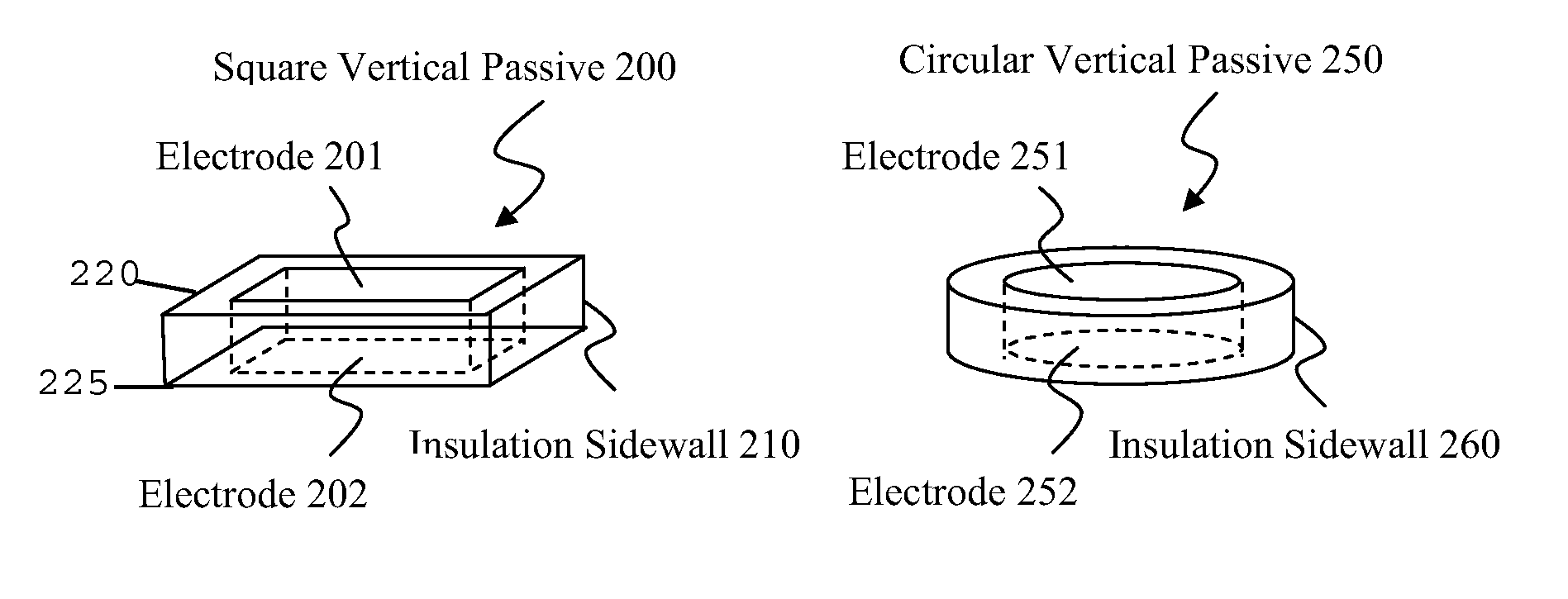
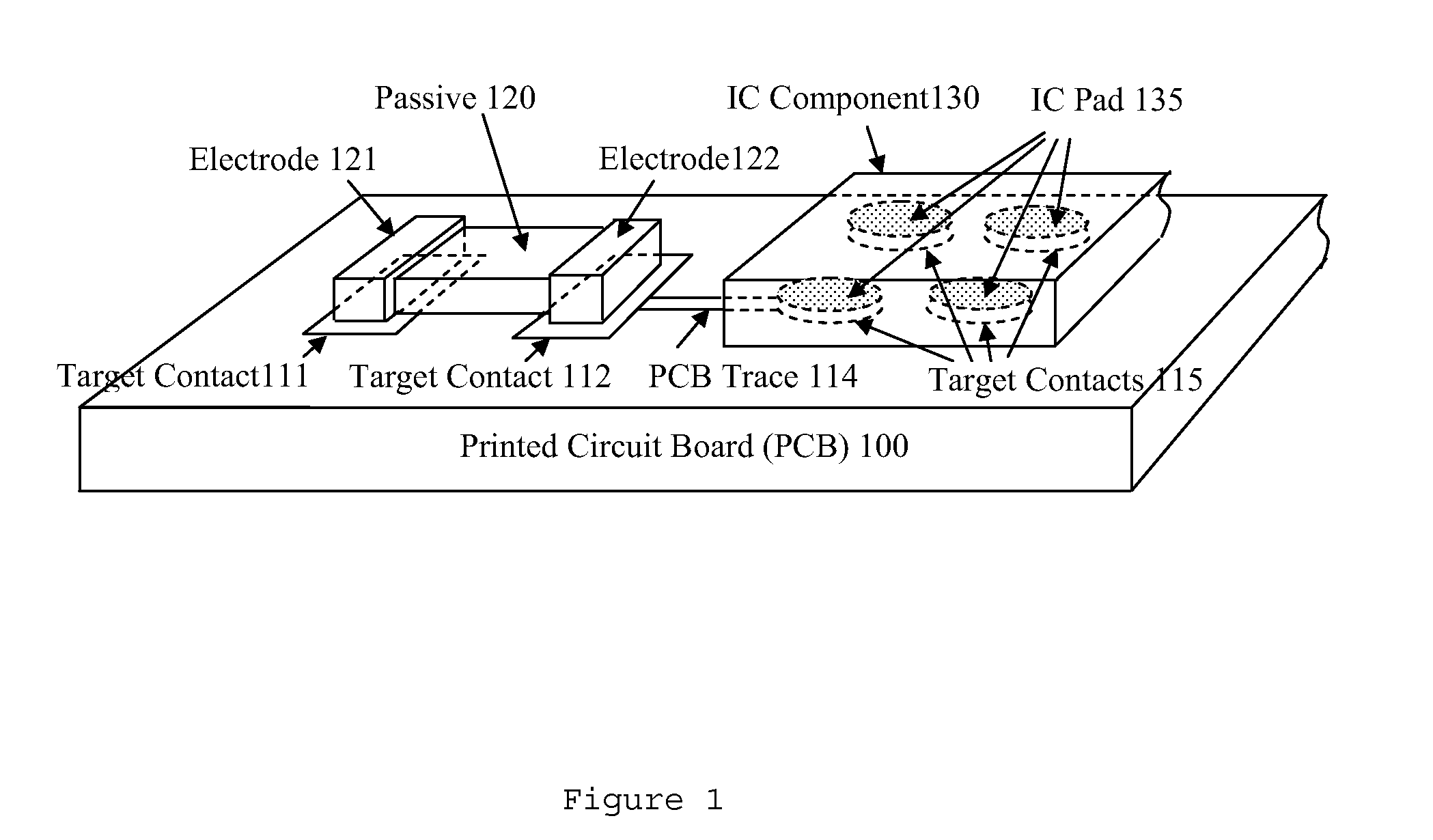
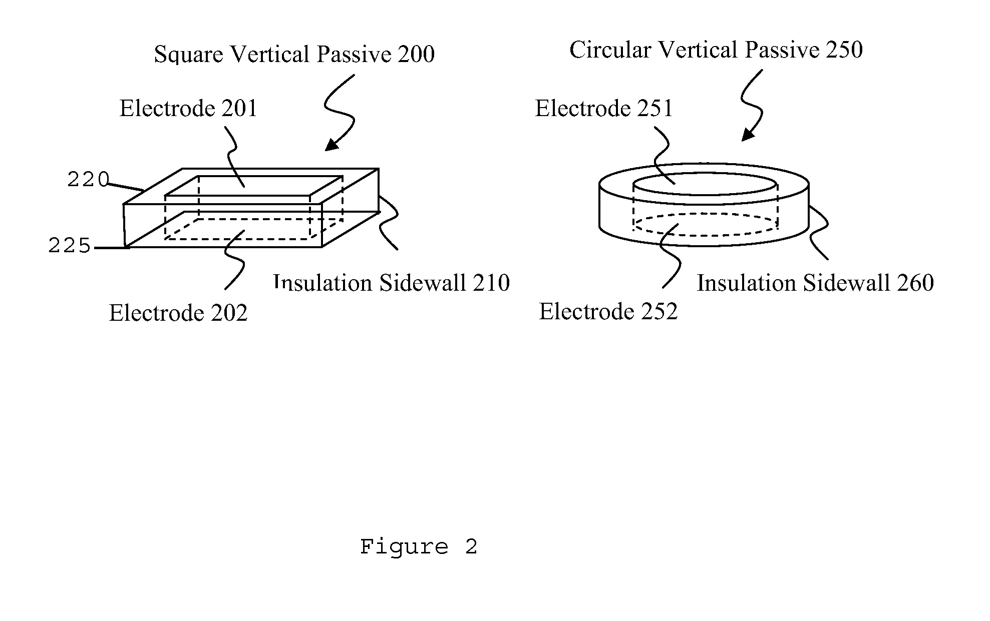
[0021]A preferred embodiment of the present invention is now described with reference to the Figures where like reference numbers indicate identical or functionally similar elements. Also in the Figures, the left most digits of each reference number correspond to the Figure in which the reference number is first used.
[0022]Reference in the specification to “one embodiment” or to “an embodiment” means that a particular feature, structure, or characteristic described in connection with the embodiments is included in at least one embodiment of the invention. The appearances of the phrase “in one embodiment” or “an embodiment” in various places in the specification are not necessarily all referring to the same embodiment.
[0023]Additionally, the language used in the specification has been principally selected for readability and instructional purposes, and may not have been selected to delineate or circumscribe the inventive subject matter. Accordingly, the disclosure of the present inve...
PUM
| Property | Measurement | Unit |
|---|---|---|
| width | aaaaa | aaaaa |
| width | aaaaa | aaaaa |
| length | aaaaa | aaaaa |
Abstract
Description
Claims
Application Information