Supercharge Your Innovation With Domain-Expert AI Agents!

Barrier coating with reduced process time

a barrier coating and process time technology, applied in the field of electronic devices, can solve the problems of undesired reaction at the electrode-organic layer interface, undesired migration, and oleds that are prone to degradation, and achieve the effects of reducing the number of barriers

Active Publication Date: 2011-04-14
GENERAL ELECTRIC CO
View PDF29 Cites 6 Cited by
  • Summary
  • Abstract
  • Description
  • Claims
  • Application Information

AI Technical Summary

Benefits of technology

The present techniques provide methods for depositing a barrier over an electronic device using both organic and inorganic materials in a controlled manner. The barrier has a low water vapor transmission rate and can protect the electronic device from adverse environmental conditions. The methods allow for the formation of the barrier in a short time, with some methods allowing for the barrier to be formed in as little as five minutes. The graded barrier consists of a combination of organic and inorganic materials, with the inorganic materials being deposited at a faster rate than the organic materials. Overall, the techniques provide a controlled and efficient way to protect electronic devices from environmental conditions.

Problems solved by technology

Light emitting structures, including OLEDs, may be prone to degradation under certain environmental conditions such as oxygen, moisture, chemicals, or other contaminants.
For example, water vapor and oxygen ingress over time may cause degradation of light emitting polymers, undesired reactions at the electrode-organic layer interfaces, corrosion of metals, or undesired migration of ionic species, etc.
Such degradation may result in the growth of dark spots, delamination, and / or the shrinking of the emissive areas of the light emitting structure.
Thus, dark spots, delamination, and / or shrinking of the emissive areas of such structures may affect the quality and / or uniformity of the image displayed.
However, such encapsulation methods may not be the most cost effective methods for sealing the structures.
However, the process time (i.e., the time required to fully encapsulate a light emitting structure) for thin film encapsulation, may be longer than the process time when using a typical glass and epoxy encapsulation process.

Method used


Image

  • Barrier coating with reduced process time
  • Barrier coating with reduced process time
  • Barrier coating with reduced process time

Examples


Embodiment Construction

[0016]One or more embodiments of the present techniques will be described below. In an effort to provide a concise description of these embodiments, not all features of an actual implementation are described in the specification. It should be appreciated that in the development of any such actual implementation, as in any engineering or design project, numerous implementation-specific decisions must be made to achieve the developers' specific goals, such as compliance with system related and business-related constraints, which may vary from one implementation to another. Moreover, it should be appreciated that such a development effort might be complex and time consuming, but would nevertheless be a routine undertaking of design, fabrication, and manufacture for one of ordinary skill having the benefit of this disclosure.

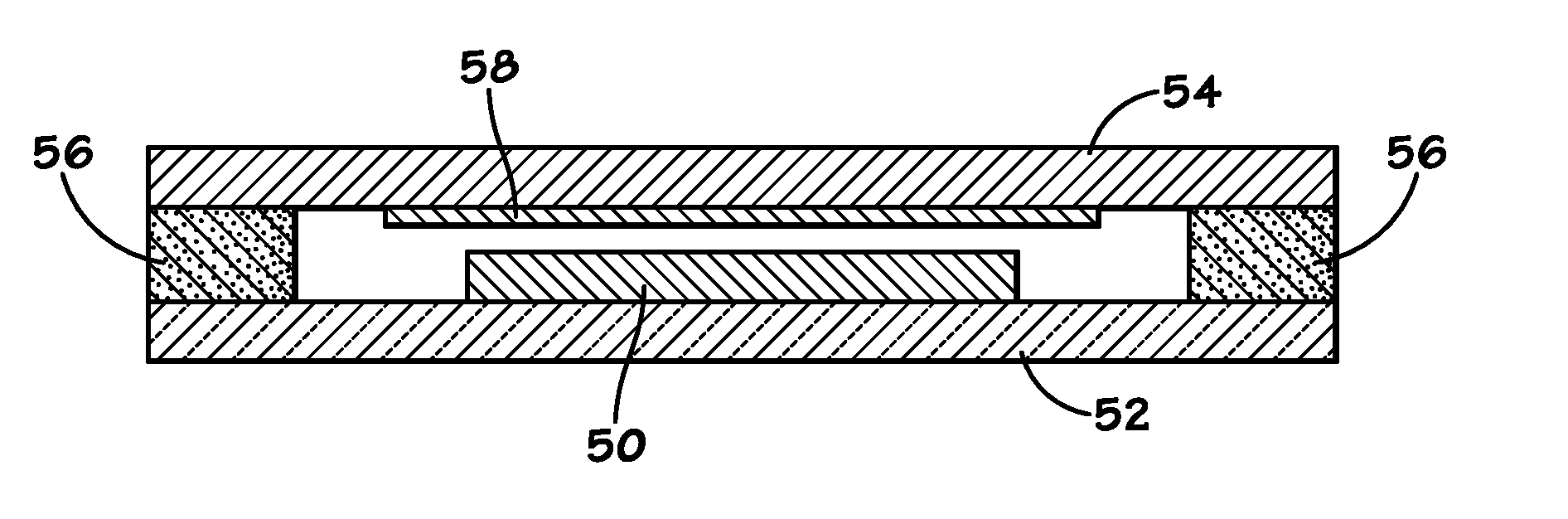
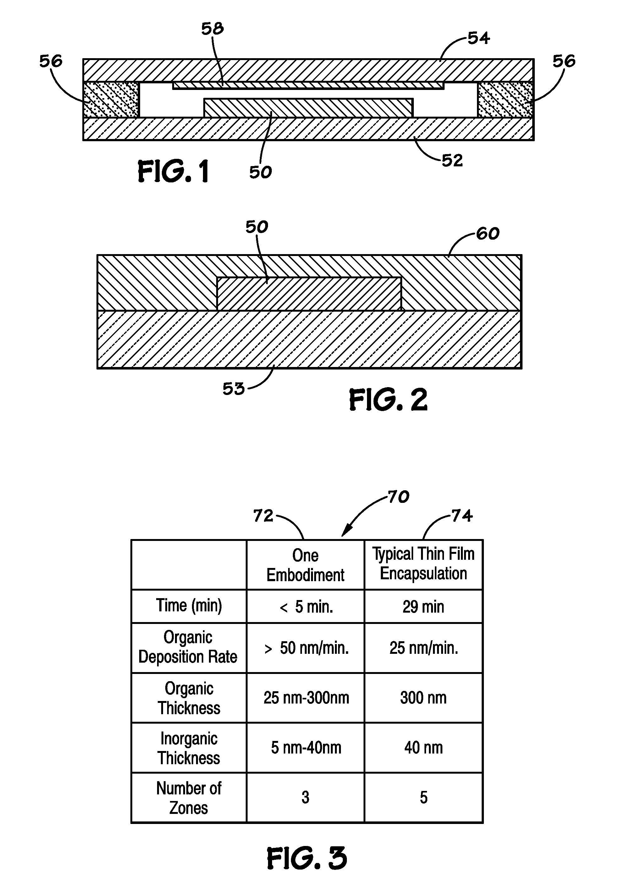
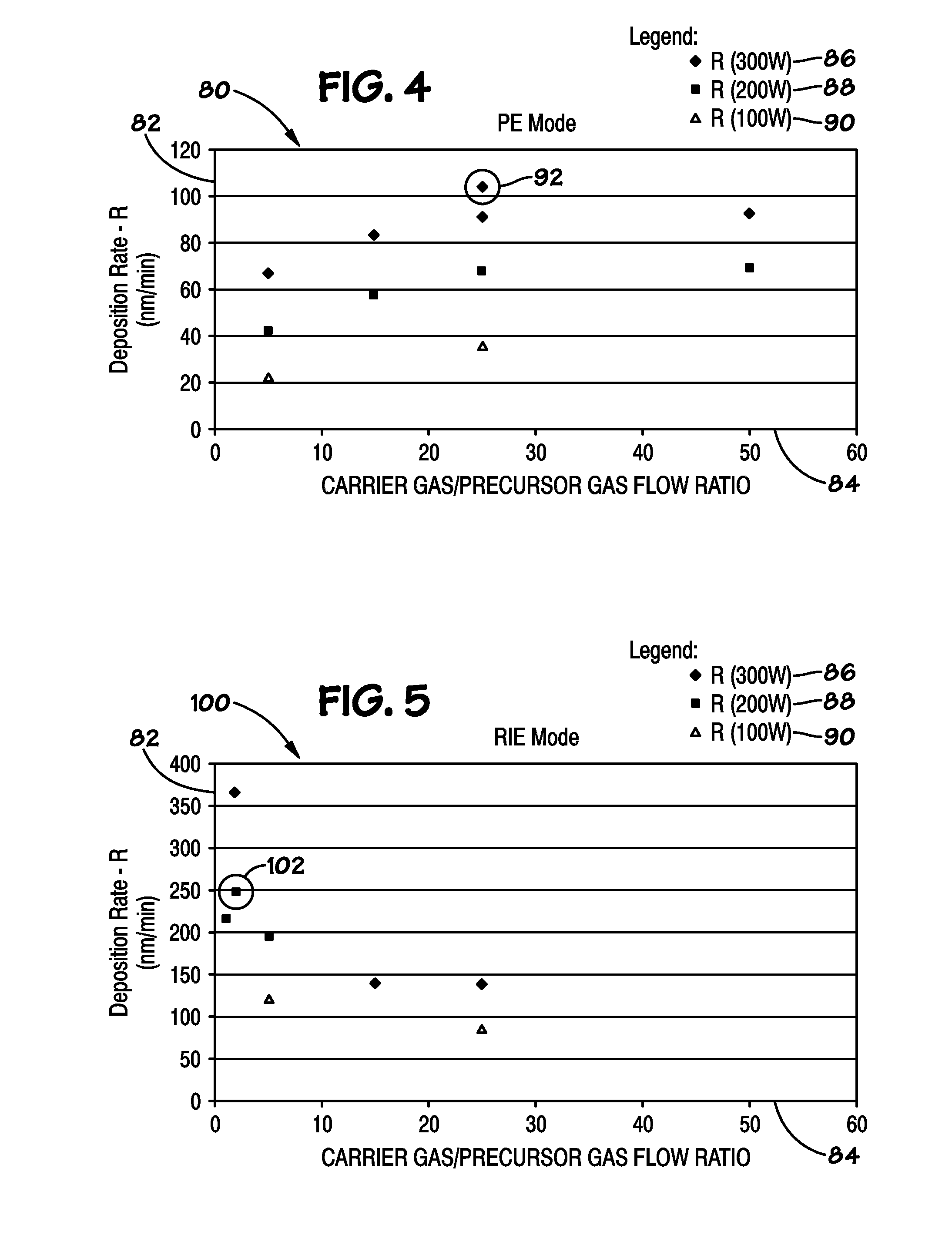
[0017]The present techniques generally relate to providing a barrier coating for a structure in an electronic device against adverse environmental conditions. For e...


PUM

PropertyMeasurementUnit
deposition rateaaaaaaaaaa
thickaaaaaaaaaa
thickaaaaaaaaaa

Abstract

The present techniques provide systems and methods for protecting electronic devices such as organic light emitting devices (OLEDs) from adverse environmental effects using a thin film encapsulation with reduced process time. In some embodiments, the process time of forming a graded barrier over the OLED structure may take less than 5 minutes, and may result in substantially similar barrier properties as those of metal and epoxy sealants and / or typical thin film encapsulations. The process time of forming the barrier may be reduced by increasing deposition rates for organic and / or inorganic materials, reducing the thicknesses of organic and / or inorganic layers, and / or varying the number of zones in the barrier.

Description

BACKGROUND[0001]The present techniques relates generally to electronic devices. More specifically, the techniques relate to methods and systems for sealing structures in electronic devices.[0002]Certain electronic devices have components that may be sensitive to adverse environmental conditions, primarily to water vapor and oxygen. For example, display devices are commonly used as screens or displays for a wide variety of electronic devices, including televisions, portable and desktop computers, and handheld devices, such as cellular telephones, personal data assistants, and media players. The display components of such devices may display images by producing patterns of light in response to electrical signals. The patterns of light, or the images and graphics formed by the display device may be formed by individual light emitting structures, such as organic light emitting diodes (OLEDs). OLEDs may be optoelectronic devices having several layers of organic materials, and may include...

Claims


Application Information

Patent Timeline
Patent Type & Authority Applications(United States)
IPC IPC(8): B05D1/36H05H1/24B05D5/12B32B9/04
CPCB05D1/60H01L2251/558H01L2251/5346H01L51/5256H10K50/8445H10K2101/80H10K2102/351
Inventor ERLAT, AHMET GUNDALAKOS, GEORGE THEODORESCHERER, BRIAN JOSEPH
Owner GENERAL ELECTRIC CO
Features
  • R&D
  • Intellectual Property
  • Life Sciences
  • Materials
  • Tech Scout
  • Unparalleled Data Quality
  • Higher Quality Content
  • 60% Fewer Hallucinations
Learn More