Data writing method for a flash memory, and controller and storage system using the same

a data writing and flash memory technology, applied in the direction of memory adressing/allocation/relocation, redundancy hardware error correction, instruments, etc., can solve the problem of higher probability of writing errors, and achieve the effect of ensuring that data is correctly written into the flash memory

Active Publication Date: 2011-04-14
PHISON ELECTRONICS
View PDF8 Cites 19 Cited by
  • Summary
  • Abstract
  • Description
  • Claims
  • Application Information

AI Technical Summary

Benefits of technology

[0011]The present invention is directed to a data writing method capable of effectively ensuring that data is correctly written into a flash memory.

Problems solved by technology

In particular, when one memory cell can store more bits of data in the MLC NAND flash memory, the probability of writing errors becomes higher.

Method used


Image

  • Data writing method for a flash memory, and controller and storage system using the same
  • Data writing method for a flash memory, and controller and storage system using the same
  • Data writing method for a flash memory, and controller and storage system using the same

Examples


first exemplary embodiment

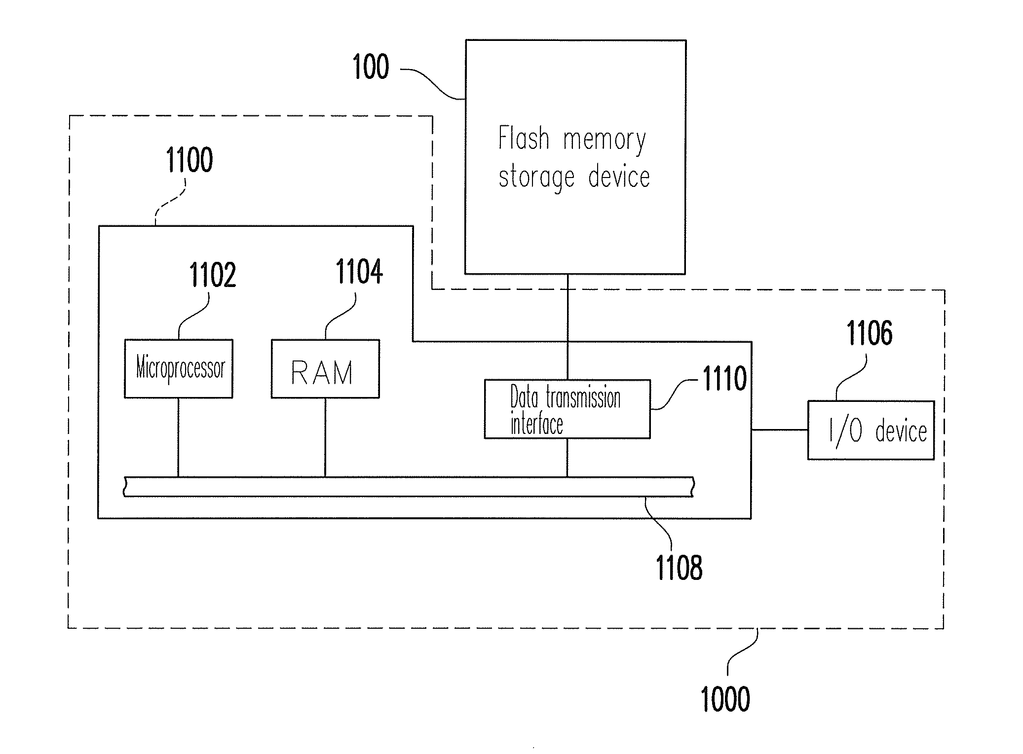
[0034]FIG. 1A is a schematic block diagram of a host system using a flash memory storage device according to a first exemplary embodiment of the present invention.

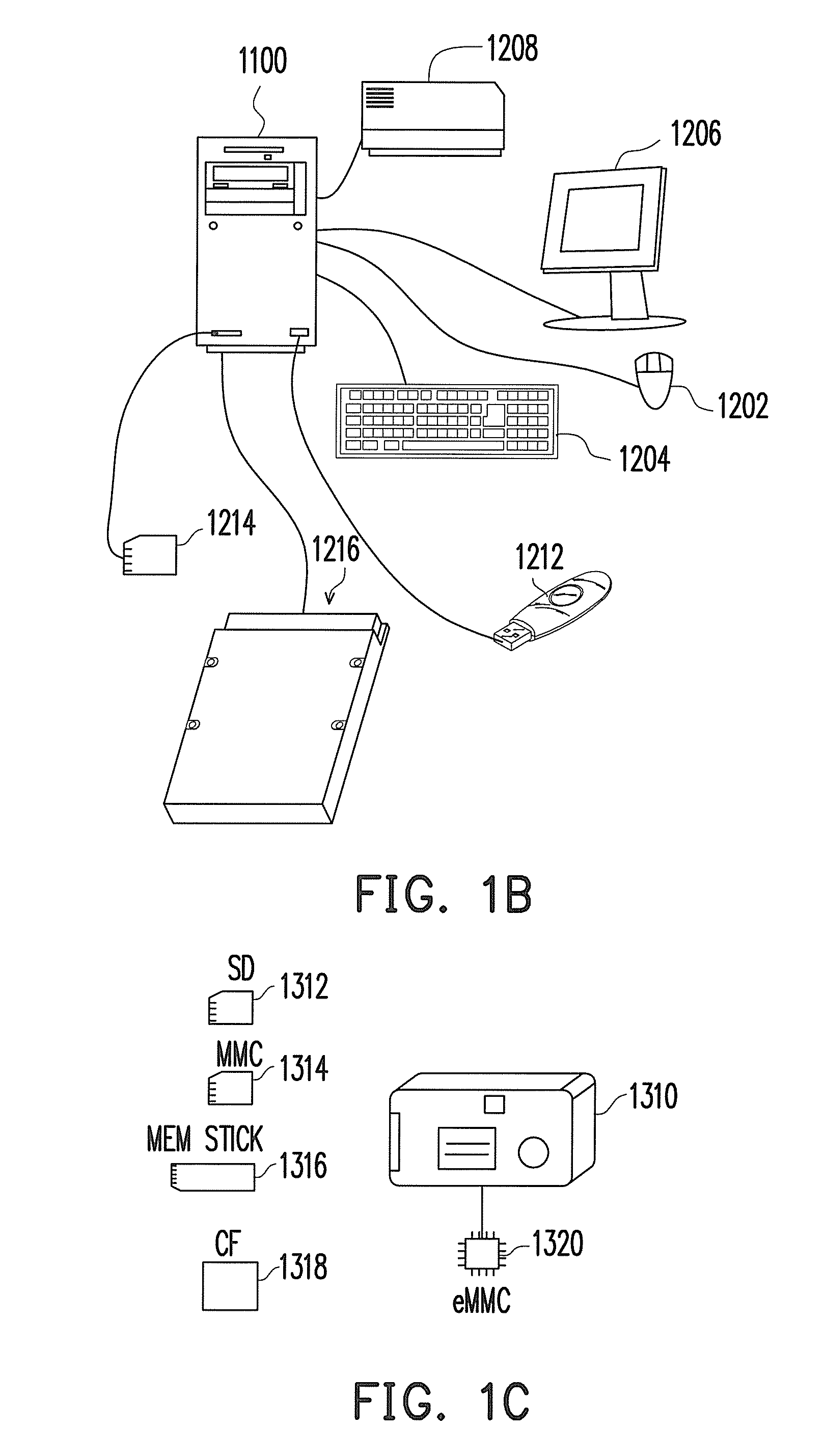
[0035]Referring to FIG. 1A, a host system 1000 includes a computer 1100 and an input / output (I / O) device 1106. The computer 1100 includes a microprocessor 1102, a random access memory (RAM) 1104, a system bus 1108, and a data transmission interface 1110. For example, the I / O device 1106 includes a mouse 1202, a keyboard 1204, a display 1206 and a printer 1208 as shown in FIG. 1B. It should be understood that the devices illustrated in FIG. 1B are not intended to limiting the I / O device 1106, and the I / O device 1106 may further include other devices.

[0036]In the present embodiment, the flash memory storage device 100 is coupled to other devices of the host system 1000 through the data transmission interface 1110. The host system 1000 can write data into or read data from the flash memory storage device 100 through the opera...

second exemplary embodiment

[0080]FIG. 6 is a schematic block diagram illustrating a flash memory storage system according to a second exemplary embodiment of the present invention.

[0081]The flash memory storage device 600 is coupled to other devices of the host system 1000 through the data transmission interface 1110. Data can be written into or read from the flash memory storage device 600 through the operations of the microprocessor 1102, the RAM 1104, and the I / O device 1106. Similarly, the flash memory storage device 600 may be the flash drive 1212, the memory card 1214, or the solid state drive (SSD) 1216 as shown in FIG. 1B, or the SD card 1312, the MMC card 1314, the memory stick 1316, the CF card 1318 or the embedded storage device 1320 (as shown in FIG. 1C). The embedded storage device 1320 includes an embedded MMC (eMMC). It should be mentioned that the eMMC is directly coupled to a substrate of the host system.

[0082]Referring to FIG. 6, the flash memory storage device 600 includes a connector 602, ...


PUM


Abstract

A data writing method for writing data from a host system into a flash memory chip is provided, and the flash memory chip have a plurality of physical blocks. The method includes receiving a host writing command and write data thereof, and executing the host writing command. The method also includes giving a data program command for writing the write data into one of the physical blocks to the flash memory chip, and giving a command for determining whether data stored in the physical block has any error bit. Accordingly, the method can effectively ensure the correctness of data to be written into the flash memory chip.

Description

CROSS-REFERENCE TO RELATED APPLICATION[0001]This application claims the priority benefit of Taiwan application serial no. 98134508, filed on Oct. 12, 2009. The entirety of the above-mentioned patent application is hereby incorporated by reference herein and made a part of this specification.BACKGROUND OF THE INVENTION[0002]1. Field of the Invention[0003]The present invention relates to a data writing method for a flash memory and particularly to a data writing method capable of effectively ensure that data is correctly written into a flash memory, and a flash memory controller and a flash memory storage system using the same.[0004]2. Description of Related Art[0005]Flash memory is the most adaptable memories to be applied in portable electronic products which are supplied power by batteries due to its data non-volatility, low power consumption, small volume, and non-mechanical structure. For example, a solid state drive (SSD) is a storage device that uses a NAND flash memory as its ...

Claims


Application Information

Patent Timeline
Patent Type & Authority Applications(United States)
IPC IPC(8): G06F11/16G06F12/00G06F12/02
CPCG06F11/1072G06F12/0246G11C2029/0411G11C29/82G11C16/10
Inventor YU, HSIANG-HSIUNGHUANG, YI-HSIANGWU, CHUNG-LINSHEN, YU-CHUNG
Owner PHISON ELECTRONICS
Why Eureka
Try Eureka