Plasma processing apparatus and plasma processing method

a plasma processing apparatus and plasma technology, applied in the field of techniques, can solve the problems of insufficient uniformity of plasma density on the substrate obtained by merely using a typical rf antenna for the plasma process, and achieve the effect of improving uniformity of the plasma process

Active Publication Date: 2011-04-28
TOKYO ELECTRON LTD
View PDF25 Cites 36 Cited by
  • Summary
  • Abstract
  • Description
  • Claims
  • Application Information

AI Technical Summary

Benefits of technology

[0023]With such configuration, especially, where the first and the second correction coil that can be coupled with the RF antenna by the electromagnetic induction are provided outside the processing chamber so as to be in parallel with the RF antenna; and the first and the second switch are provided in the loop of the first and the second correction soil and the opening / closing (on / off) state thereof is controlled, it is possible to stably obtain in a standardized manner the effect of the correction coil on the RF magnetic field generated around the antenna conductor by the RF current flowing in the RF antenna when the RF power is supplied from the RF power supply unit to the RF antenna (the effect of locally decreasing the density of the plasma generated by the inductive coupling near the position overlapped with the coil conductor). Accordingly, the plasma density distribution near the substrate on the substrate supporting unit can be arbitrarily and accurately controlled, and the uniformity of the plasma process can be easily improved.

Problems solved by technology

However, the uniformity of the plasma density on the substrate that is obtained by merely using a typical RF antenna is generally insufficient for the plasma process.

Method used


Image

  • Plasma processing apparatus and plasma processing method
  • Plasma processing apparatus and plasma processing method
  • Plasma processing apparatus and plasma processing method

Examples


first embodiment

[0058]A first embodiment of the present invention will be described with reference to FIGS. 1 to 10.

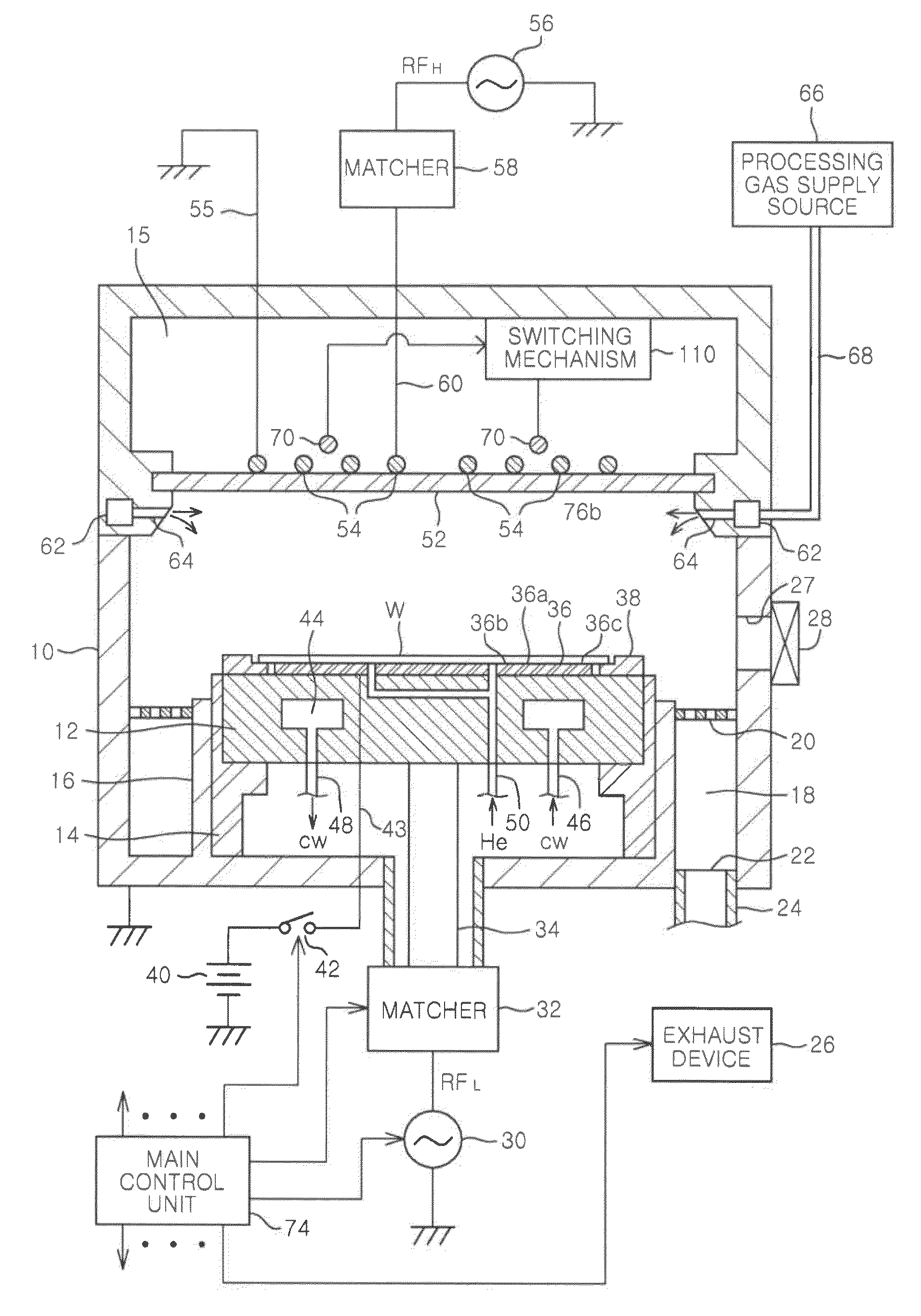
[0059]FIG. 1 shows a configuration of an inductively coupled plasma processing apparatus in accordance with the first embodiment of the present invention. The inductively coupled plasma processing apparatus is configured as a plasma etching apparatus using a planar coil type RF antenna, and includes a cylindrical vacuum chamber (processing chamber) 10 made of a metal, e.g., aluminum, stainless steel or the like. The chamber 10 is frame-grounded.

[0060]In the inductively coupled plasma etching apparatus, various units having no involvement in plasma generation will be described first.

[0061]At a lower central portion of the chamber 10, a circular plate-shaped susceptor 12 for mounting thereon a target substrate, e.g., a semiconductor wafer W as a substrate supporting table is horizontally arranged. The susceptor 12 also serves as an RF electrode. The susceptor 12, which is made of, e.g.,...

second embodiment

[0113]Hereinafter, a second embodiment of the present invention will be described with reference to FIGS. 11 to 14.

[0114]FIG. 11 shows a configuration of an inductively coupled plasma etching apparatus in accordance with the second embodiment of the present invention. In FIG. 11, like reference numerals are used for like parts having the same configurations or functions as those of the apparatus of the first embodiment (see FIG. 1).

[0115]The characteristics of the second embodiment are different from those of the first embodiment in that a resistance varying mechanism 120 is provided instead of the switching mechanism 110.

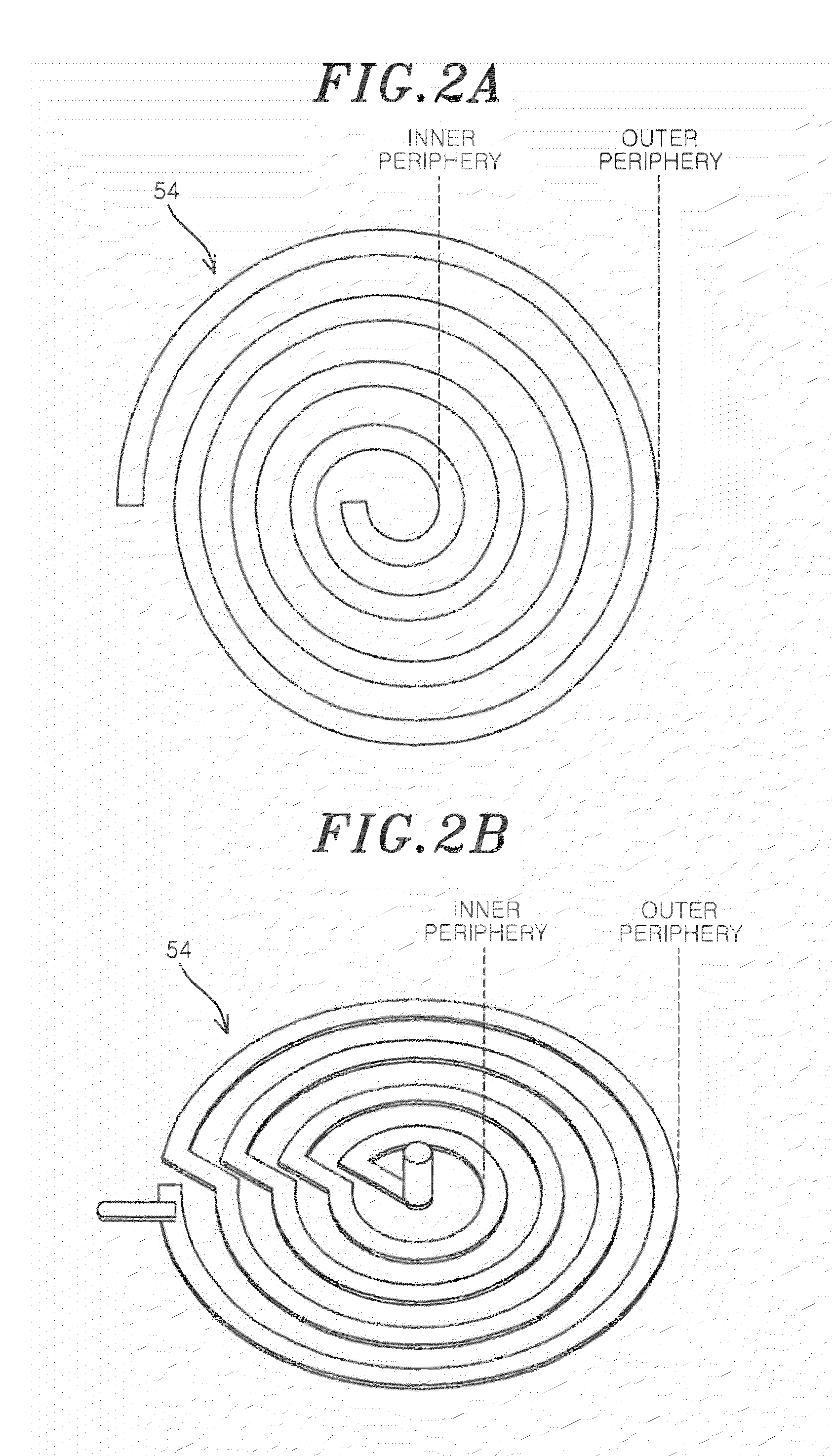
[0116]More specifically, the correction coil 70 is formed of a single- or multi-wound coil having open ends with a gap g therebetween, and is arranged to be concentric with the RF antenna 54 such that its coil conductor is diametrically positioned between the inner periphery and the outer periphery of the RF antenna 54 (preferably, around the middle portion therebe...

third embodiment

[0139]In a third embodiment, the switching mechanism 110 of the first embodiment can be replaced with an opening / closing mechanism 150 shown in FIG. 18. The opening / closing mechanism 150 includes a switch 152 connected to both open ends of the correction coil 70 via conductors, and an opening / closing control circuit 154 for switching-controlling the opening / closing (on / off) state of the switch 152 based on the instruction from the main control unit 74.

[0140]In the opening / closing mechanism 150, when the switch 152 is switched to the open (off) state, the induced current does not flow in the correction coil 70, which is equivalent to the case where the correction coil 70 is not provided. When the switch 152 is switched to the closed (on) state, the correction coil 70 becomes equivalent to a coil having both closed ends, and the induced current flows in the correction coil 70 by allowing the current of the RF power RFH to flow in the RF antenna 54.

[0141]As shown in FIG. 19, the openin...


PUM

PropertyMeasurementUnit
frequencyaaaaaaaaaa
outer radiusaaaaaaaaaa

Abstract

A plasma processing apparatus includes a processing chamber including a dielectric window; a coil-shaped RF antenna, provided outside the dielectric window; a substrate supporting unit provided in the processing chamber; a processing gas supply unit; an RF power supply unit for supplying an RF power to the RF antenna to generate a plasma of the processing gas by an inductive coupling in the processing chamber, the RF power having an appropriate frequency for RF discharge of the processing gas; a correction coil, provided at a position outside the processing chamber where the correction coil is to be coupled with the RF antenna by an electromagnetic induction, for controlling a plasma density distribution on the substrate in the processing chamber; a switching device provided in a loop of the correction coil; and a switching control unit for on-off controlling the switching device at a desired duty ratio by pulse width modulation.

Description

CROSS-REFERENCE TO RELATED APPLICATIONS[0001]This application claims priority to Japanese Patent Application Nos. 2009-245988 and 2009-245991 filed on Oct. 27, 2009 and 2010-215113 filed on Sep. 27, 2010 and U.S. Provisional Application Nos. 61 / 265,545 and 61 / 265,523 filed on Dec. 1, 2009, the entire contents of which are incorporated herein by reference.FIELD OF THE INVENTION[0002]The present invention relates to a technique for performing a plasma process on a target substrate to be processed; and, more particularly, to an inductively coupled plasma processing apparatus and a plasma processing method therefor.BACKGROUND OF THE INVENTION[0003]In the manufacturing process of a semiconductor device or a flat panel display (FPD), a plasma is widely used in a process such as etching, deposit, oxidation, sputtering or the like since it has a good reactivity with a processing gas at a relatively low temperature. In such plasma process, the plasma is mostly generated by a radio frequency ...

Claims


Application Information

Patent Timeline
Patent Type & Authority Applications(United States)
IPC IPC(8): C23F1/08C23C16/52C23C16/455C23C16/458C23C16/505C23F1/00
CPCH01J37/321H01L21/67109H01J37/32146H01J37/3211H01L21/6831H01J37/32174H05H1/46H05H1/4652
Inventor YAMAZAWA, YOHEIKOSHIMIZU, CHISHIOSAITO, MASASHIDENPOH, KAZUKIYAMAWAKU, JUN
Owner TOKYO ELECTRON LTD
Why Eureka
Try Eureka