

Plasma processing system with locally-efficient inductive plasma coupling
a plasma processing system and local-efficient technology, applied in the direction of vacuum evaporation coating, coating, electric discharge tube, etc., can solve the problem of intense capacitive coupling between the antenna and the plasma processing system, the geometry of the sputtering target affects the uniformity of the coating on the wafer, and the power is enormously increased to provide identical plasma conditions for etching or deposition, etc. problem, to achieve the effect of improving the uniformity of plasma processing
- Summary
- Abstract
- Description
- Claims
- Application Information
AI Technical Summary
Benefits of technology
Problems solved by technology
Method used
Image

Examples
Embodiment Construction
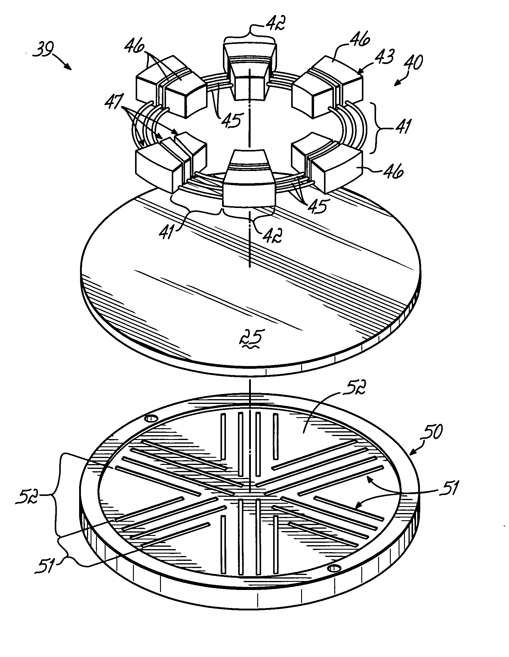
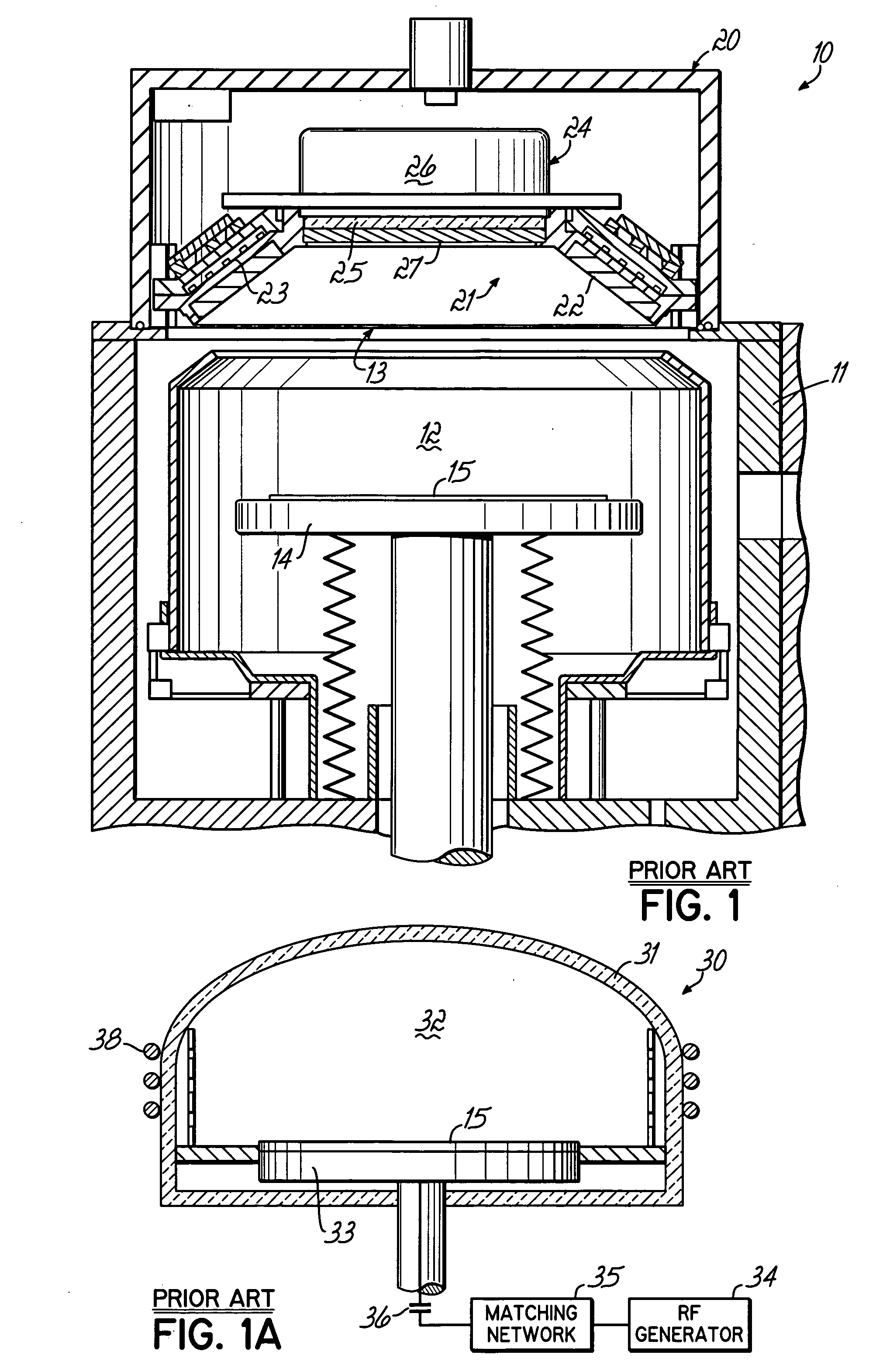
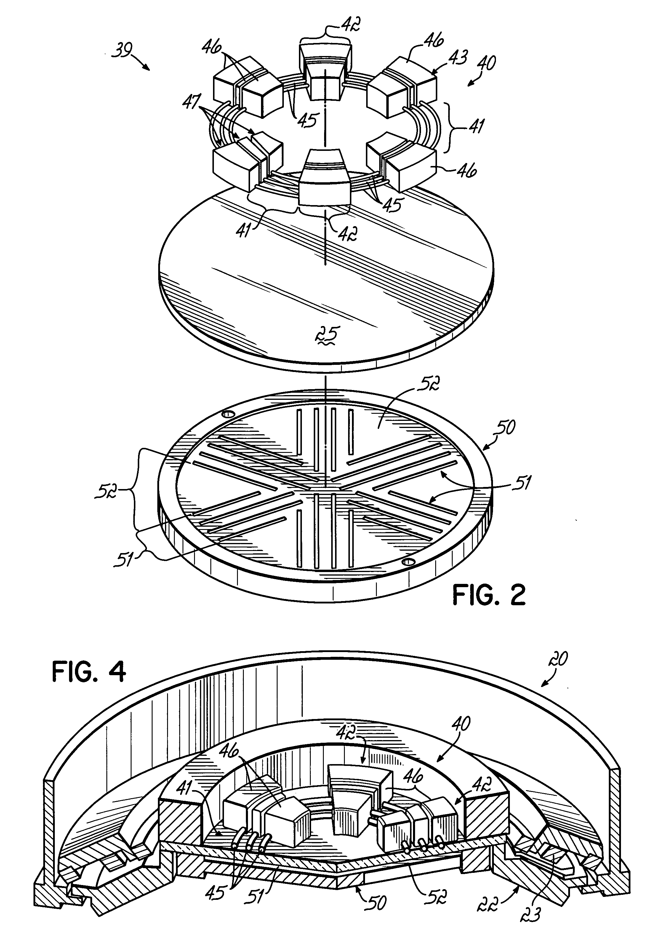
[0061] The ICP source of the present invention can be used in various plasma processing systems, such as those for performing sputter etching and deposition processes, plasma-enhanced CVD (PECVD) processes, ionized PVD (iPVD) processes, and reactive ion etching processes (RIE). FIG. 1 illustrates an iPVD apparatus 10 of a type for the manufacture of semiconductor wafers in which embodiments of the invention are described below. Examples of semiconductor wafer processing machines of the iPVD type are described in U.S. Pat. Nos. 6,080,287 and 6,287,435, both hereby expressly incorporated by reference herein.
[0062] The iPVD apparatus 10 includes a vacuum processing chamber 12 enclosed in a chamber wall 11 having an opening 13 at the top thereof in which is mounted an ionized sputtering material source 20, which seals the opening 13 to isolate the vacuum within the chamber 12 from external ambient atmosphere. Within the chamber 12 is a wafer support 14 that holds a semiconductor wafer ...
PUM
| Property | Measurement | Unit |
|---|---|---|
| diameters | aaaaa | aaaaa |
| diameters | aaaaa | aaaaa |
| diameter | aaaaa | aaaaa |
Abstract
Description
Claims
Application Information