Solid-state imaging device, method of manufacturing solid-state imaging device, and electronic equipment
- Summary
- Abstract
- Description
- Claims
- Application Information
AI Technical Summary
Benefits of technology
Problems solved by technology
Method used
Image

Examples
first embodiment
1. First Embodiment
(A) Device Configuration
(A-1) Principal Part Configuration of Camera
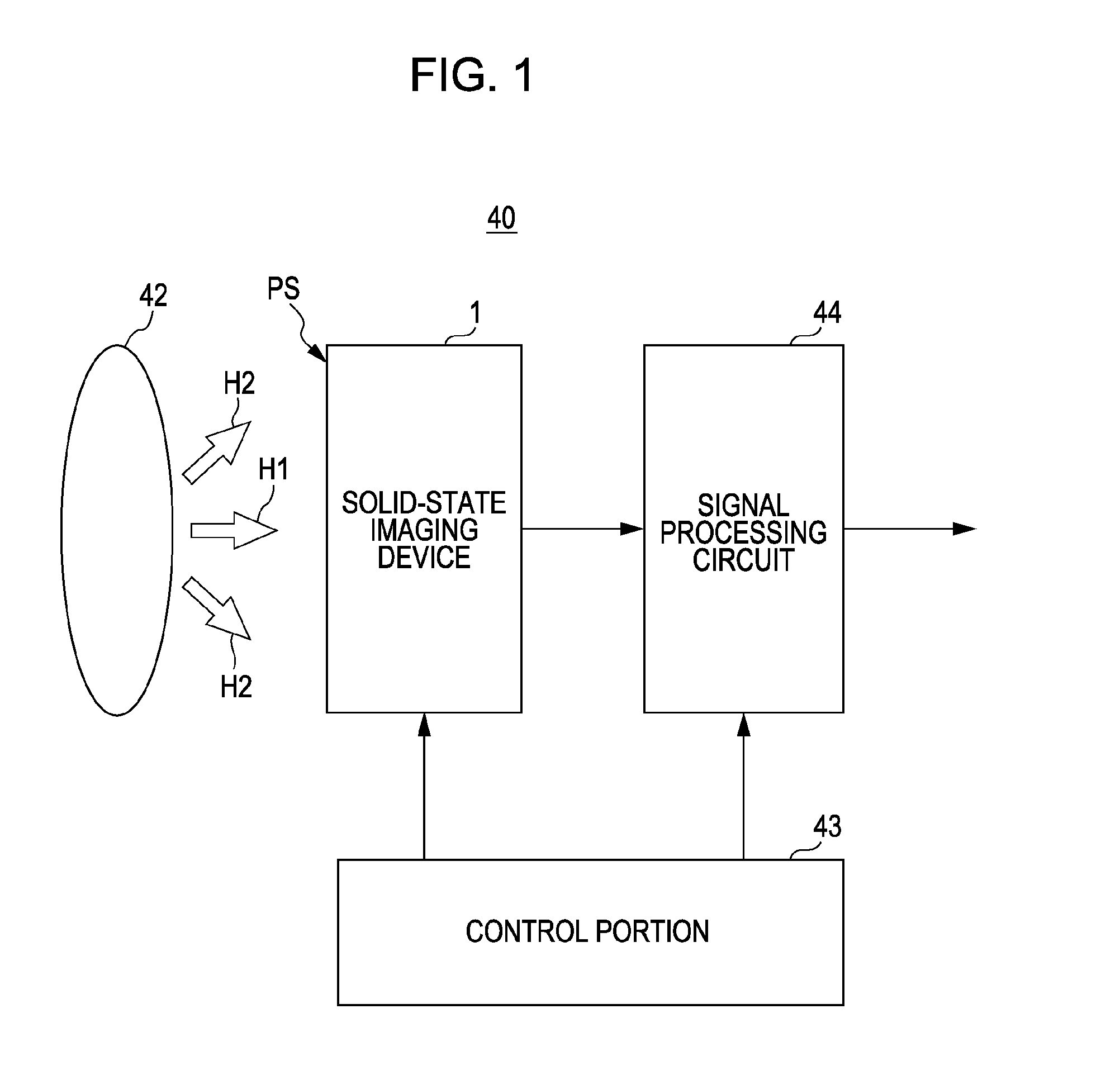
[0076]FIG. 1 is a configuration diagram illustrating a configuration of a camera 40 in a first embodiment relating to the present invention.
[0077]As shown in FIG. 1, the camera 40 has a solid-state imaging device 1, an optical system 42, a control portion 43, and a signal processing circuit 44. Each portion will be sequentially described.
[0078]The solid-state imaging device 1 creates a signal electric charge by receiving light (subject image), which is incident via the optical system 42, at a capturing surface PS and performing the photoelectric transformation. Herein, the solid-state imaging device 1 is driven based on the control signal that is output from the control portion 43. Specifically, the signal electric charge is read and output as low data.
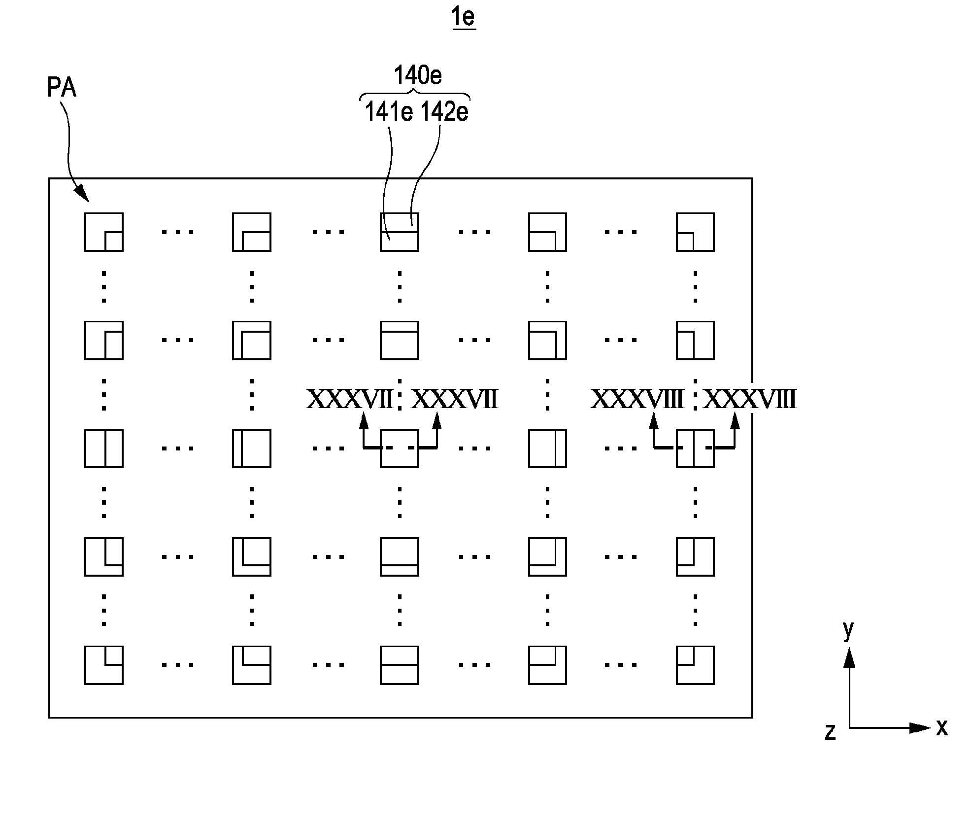
[0079]In the present embodiment, as shown in FIG. 1, in the solid-state imaging device 1, in a center portion of the capturing surface PS, a main r...
second embodiment
2. Second Embodiment
(A) Device Configuration
[0215]FIGS. 13 and 14 are drawings illustrating the principal parts of a solid-state imaging device 1b in a second embodiment relating to the present invention.
[0216]Herein, similarly to FIG. 5, FIG. 13 illustrates the cross section of the capturing area PA. Similarly to FIG. 7FIG. 14 illustrates an upper surface of a micro lens 140b.
[0217]As shown in FIGS. 13 and 14, in the present embodiment, the micro lens 140b is different from that of the first embodiment. The present embodiment is the same as the first embodiment except for this. For this reason, description of the overlapping portions will be omitted.
[0218]As shown in FIGS. 13 and 14, the micro lens 140b includes the first refractive index layer 141 and the second refractive index layer 142b.
[0219]In addition, as shown in FIG. 13, the micro lens 140b is configured so that the vertical cross section which is the surface (xz surface) perpendicular to the capturing surface (xy surfac...
third embodiment
3. Third Embodiment
(A) Device Configuration
[0236]FIGS. 16 and 17 are diagrams illustrating the principal parts of a solid-state imaging device 1c in a third embodiment relating to the invention.
[0237]Herein, similarly to FIG. 5, FIG. 16 illustrates the cross section of the capturing area PA. Similarly to FIG. 7, FIG. 17 illustrates the upper surface of the micro lens 140c.
[0238]As shown in FIGS. 16 and 17, in the present embodiment, the micro lens 140c is different from that of the first embodiment. Except for this point, the present invention is the same as the first embodiment. For this reason, description of the overlapped portions will be omitted.
[0239]As shown in FIGS. 16 and 17, the micro lens 140c includes the first refractive index layer 141c and the second refractive index layer 142.
[0240]As shown in FIG. 16, the micro lens 140c is configured so that the vertical cross section which is a surface (xz surface) perpendicular to the capturing surface (xy surface) is a rectangu...
PUM
 Abstract
Description
Claims
Application Information
 - Generate Ideas
- Intellectual Property
- Life Sciences
- Materials
- Tech Scout
- Unparalleled Data Quality
- Higher Quality Content
- 60% Fewer Hallucinations
Browse by: Latest US Patents, China's latest patents, Technical Efficacy Thesaurus, Application Domain, Technology Topic, Popular Technical Reports.
© 2025 PatSnap. All rights reserved.Legal|Privacy policy|Modern Slavery Act Transparency Statement|Sitemap|About US| Contact US: help@patsnap.com