

Photovoltaic Power Converter
a power converter and photovoltaic technology, applied in the field of devices, can solve the problems of limited light conversion efficiency, more than half of the optical power of incident light lost, and low light conversion efficiency
- Summary
- Abstract
- Description
- Claims
- Application Information
AI Technical Summary
Problems solved by technology
Method used
Image

Examples
Embodiment Construction
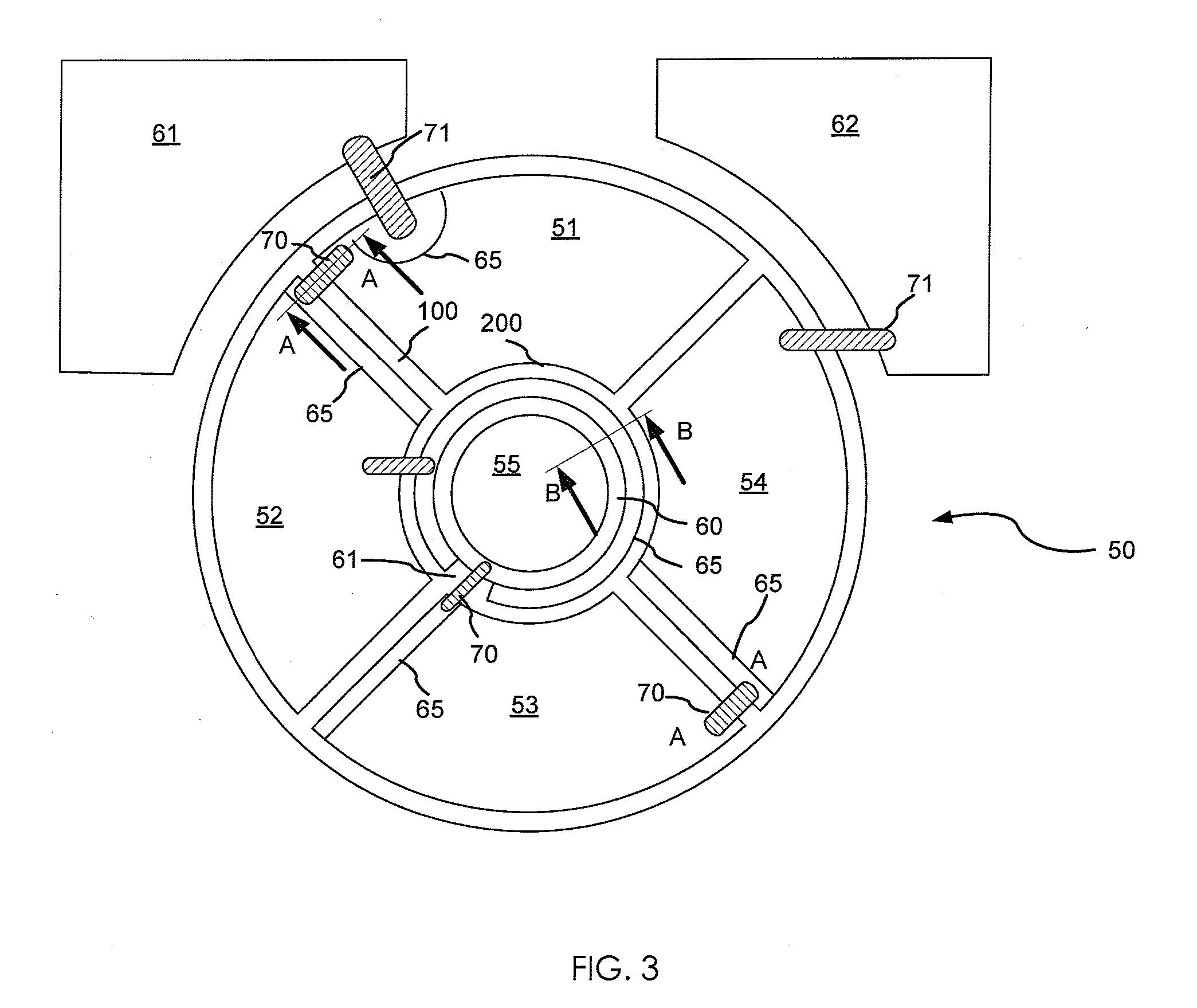
[0030]Exemplary embodiments of the photovoltaic power converter (PPC) of the present invention will now be first described with reference to FIGS. 3, 4 and 5.
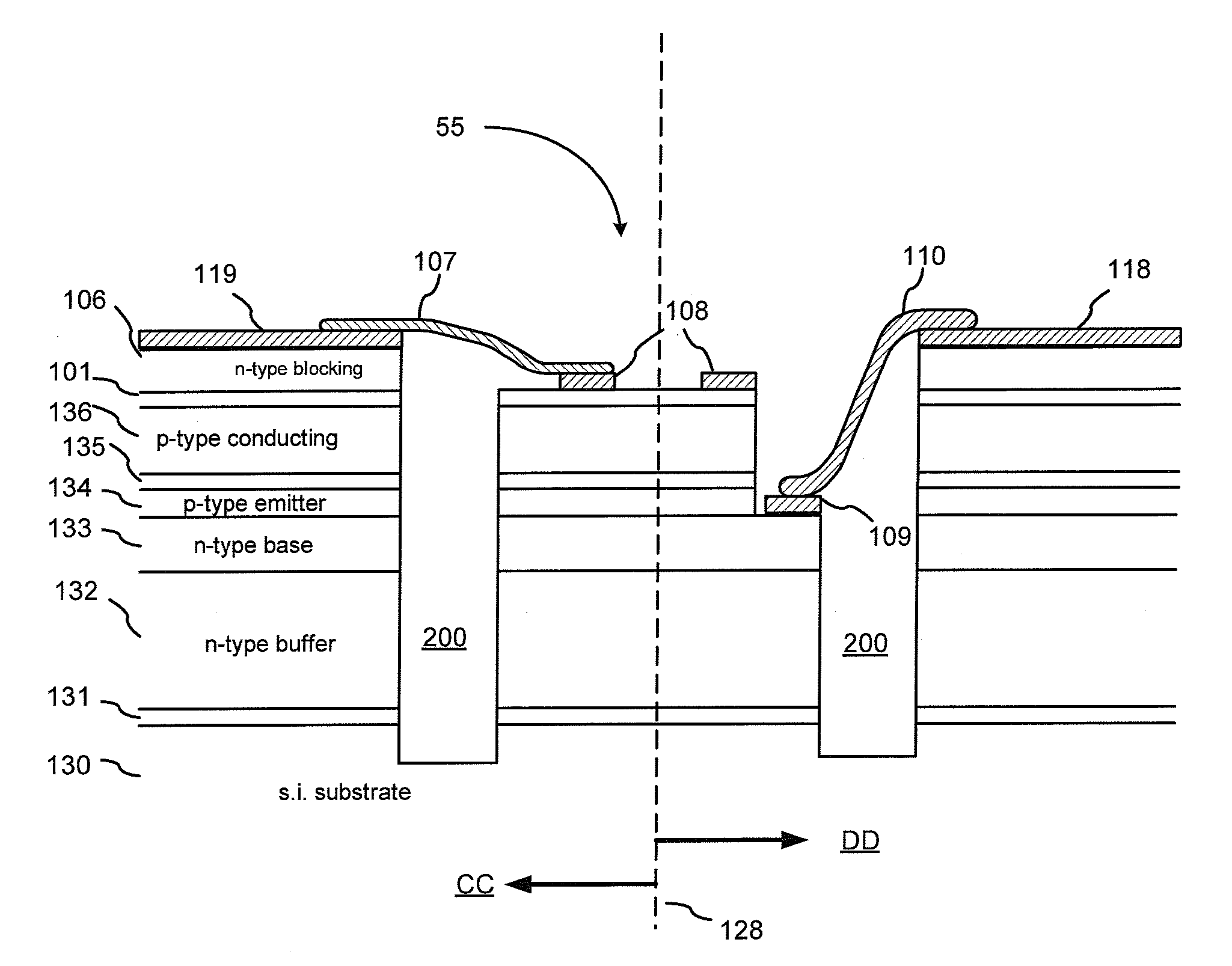
[0031]Referring first to FIG. 3, the PPC 50 includes a plurality of device segments 51-55 arranged in a circular pattern, with a central portion, or segment 55 and a plurality of segments 51-54 that are disposed around the central segment 55 surrounding said central segment and forming a ring-like structure. The segments 51-54, which will also be referred to herein as the ring segments, and the central segment 55 are separated from each other by narrow trenches 100, 200. A circular, or more generally, endless trench 200 separates the central segment 55 from the ring segments 51-54, while the trenches 100 extend radially therefrom to separate the ring sections 51-54 from each other. The trenches 100, 200 are etched in an epitaxially grown semiconductor wafer using one of known in the art etching techniques for etching high aspec...
PUM
 Abstract
Description
Claims
Application Information