Method and system for manufacturing microstructure in photosensitive glass substrate

a technology of photosensitive glass and microstructure, which is applied in the direction of polycrystalline material growth, crystal growth process, chemistry apparatus and processes, etc., can solve the problems of inconvenient use, time-consuming, and insufficient heat treatment of photosensitive glass substrates, so as to reduce steps and time, high alignment precision, and high precision

Inactive Publication Date: 2011-05-12
IND TECH RES INST
View PDF16 Cites 29 Cited by
  • Summary
  • Abstract
  • Description
  • Claims
  • Application Information

AI Technical Summary

Benefits of technology

Compared with the prior art, second femtosecond laser pulses of the present invention that have a frequency higher than that of the femtosecond laser pulses used to form the modified region is focused on the modified region to perform a local tempering treatment, such that the unmodified region of the present invention does not deform due to the heating. Moreover, an ideal

Problems solved by technology

However, common exposure and development processes can only form microstructures on the surfaces of the photosensitive glass substrates; and, when performing the temper treatment in the heating furnace, unnecessary deformation happens in the unmodified regions of the photosensitive glass substrates due to heating.
In addition, it takes several hours to perform the temper treatment in the heating furnace.
That is inconvenient in use and is time-cons

Method used


Image

  • Method and system for manufacturing microstructure in photosensitive glass substrate
  • Method and system for manufacturing microstructure in photosensitive glass substrate
  • Method and system for manufacturing microstructure in photosensitive glass substrate

Examples


example 1

Manufacture of Surface Microstructure in Photosensitive Glass Substrate

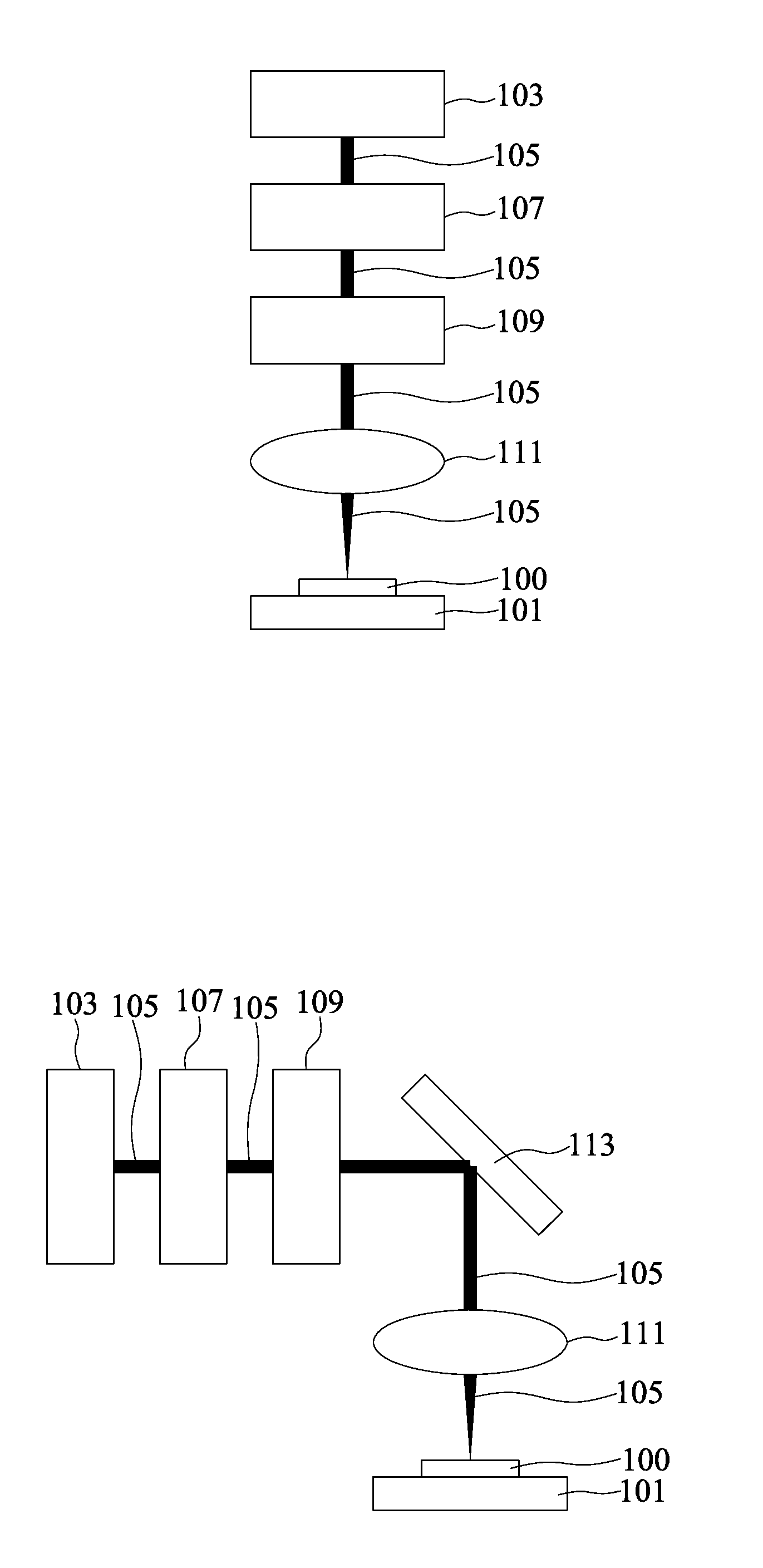
In this example, the femtosecond laser pulses with a frequency of 1 kHz and energy of 0.2 mW were focused on the surface of a photosensitive glass substrate by a 10× objective lens to modify the surface with a scanning speed of 0.05 mm / s to define a modified region. Then, the second femtosecond laser pulses with a frequency of 80 MHz and energy of 300 mW were focused on the surface of the photosensitive glass substrate by a 50× objective lens and the second focused femtosecond laser pulses scanned the modified region of the photosensitive glass substrate with a speed of 0.5 mm / s for the tempering treatment. Finally, the crystallized region was removed by 8% of hydrofluoric acid accompanied with ultrasonic vibration for 15 minutes.

As shown in FIG. 3A, the position circled by the dotted line A shows that a groove is formed by the method of Example 1. However, as shown in FIG. 3B, if tempering is performed by femtos...

example 2

Manufacture of Blind Via of Photosensitive Glass Substrate

In this example, femtosecond laser pulses with a frequency of 1 kHz and energy of 0.255 mW were focused on the interior of a photosensitive glass substrate by a 10× objective lens for modification, wherein, as shown in FIG. 4, in order to form modified regions of pits 402 at two positions of the surface of the photosensitive glass substrate 400, the femtosecond laser pulses scanned from the surface of the photosensitive glass substrate down to a depth (D) of 0.2 mm at the predetermined two ends of a blind via at a speed less than 0.5 mm / s, such as 0.05 mm / s. The micro-channel 404 connected between the pits 402 of the photosensitive glass substrate was scanned by a speed of 0.5 mm / s to form a U-shaped modified region. Then, the femtosecond laser pulses with a frequency of 80 MHz and energy of 330 mW were focused on the interior of the photosensitive glass substrate by a 50× objective lens and scanned the modified region of the...


PUM

PropertyMeasurementUnit
Timeaaaaaaaaaa
Poweraaaaaaaaaa
Poweraaaaaaaaaa

Abstract

The present invention provides a method and system for manufacturing a microstructure in a photosensitive glass substrate, which include the steps of generating first femtosecond laser pulses by a femtosecond laser source and focusing the first femtosecond laser pulses on a surface or an interior of the photosensitive glass substrate by a focus lens to define a modified region; generating second femtosecond laser pulses by the femtosecond laser source, adjusting a frequency of the second femtosecond laser pulses to be higher than that of the first femtosecond laser pulses by a frequency adjustment unit and an energy adjustment unit; focusing the adjusted second femtosecond laser pulses on the modified region of the photosensitive glass substrate to crystallize a substance of the modified region; and, after crystallization, etching off the crystallized region to obtain the microstructure in the photosensitive glass substrate.

Description

TECHNICAL FIELDThe present invention relates to the manufacture of a microstructure in a photosensitive glass substrate, and more particularly to a method and a system for manufacturing a microstructure in a photosensitive glass substrate by a femtosecond laser.BACKGROUNDPhotosensitive glass is substance with high transparency, high hardness, high chemical resistance and high heat resistance. Because the glass is doped with specific metal elements, the absorbance thereof to radiation with a wavelength between 250 to 350 nm is high. Therefore, the photosensitive glass is usually used in the manufacture of biochips and glass inserts.To manufacture microstructures on surfaces of the photosensitive glass substrates, the typical process includes the following steps: modifying specific regions of the photosensitive glass substrates by exposure and development processes; tempering the entire photosensitive glass substrates in a heating furnace to produce crystals in the modified regions; a...

Claims


Application Information

Patent Timeline
IPC IPC(8): B44C1/22C23F1/08
CPCC03C15/00C30B29/34C30B1/023C03C23/0025
Inventor CHIEN, CHIH-WEICHENG, CHUNG-WEILI, PING-XIANGCHEN, JENG-SHYONG
Owner IND TECH RES INST
Why Eureka
Try Eureka