Input circuit

a technology of input circuit and input signal, which is applied in the field of input circuit, can solve the problems of reducing response speed, power supply voltage dependence, and inability of input circuit to receive input signals with small swing width, so as to prevent the reduction of response speed, reduce the ratio of on-state resistance of pmos transistor to on-state resistance of nmos transistor, and increase the hysteresis voltage

Inactive Publication Date: 2011-05-12
SEIKO INSTR INC
View PDF8 Cites 3 Cited by
  • Summary
  • Abstract
  • Description
  • Claims
  • Application Information

AI Technical Summary

Benefits of technology

[0015]The present invention is capable of ensuring a large hysteresis voltage in a wide range of power supply voltage conditions without using a logic circuit, an operational amplifier circuit, or the like. Besides, a ratio of an ON-state resistance of an NMOS transistor to an ON-state resistance of a PMOS transistor may be reduced as compared with the conventional technologies, to thereby prevent a response speed from reducing during low power supply voltage operation. Further, as compared with the conventional circuits, hysteresis characteristics to be obtained are less dependent on the power supply voltage, and hence it is possible to make design without increasing a circuit scale.
[0016]As described above, the input circuit according to the present invention provides an effect of, as compared with the conventional technologies, suppressing the power supply voltage dependence of the hysteresis voltage and the response speed without increasing the circuit scale.

Problems solved by technology

In the conventional technologies, however, such hysteresis voltage and response speed suffer from the power supply voltage dependence as described below.
As described above, a high circuit threshold makes it impossible for the input circuit to receive an input signal with a small swing width.
In addition, under the condition of low power supply voltage, the current drivability of the NMOS transistor 901 is lower than those of the PMOS transistors, with the result that the response speed reduces under the condition of low power supply voltage.

Method used


Image

  • Input circuit
  • Input circuit
  • Input circuit

Examples


first embodiment

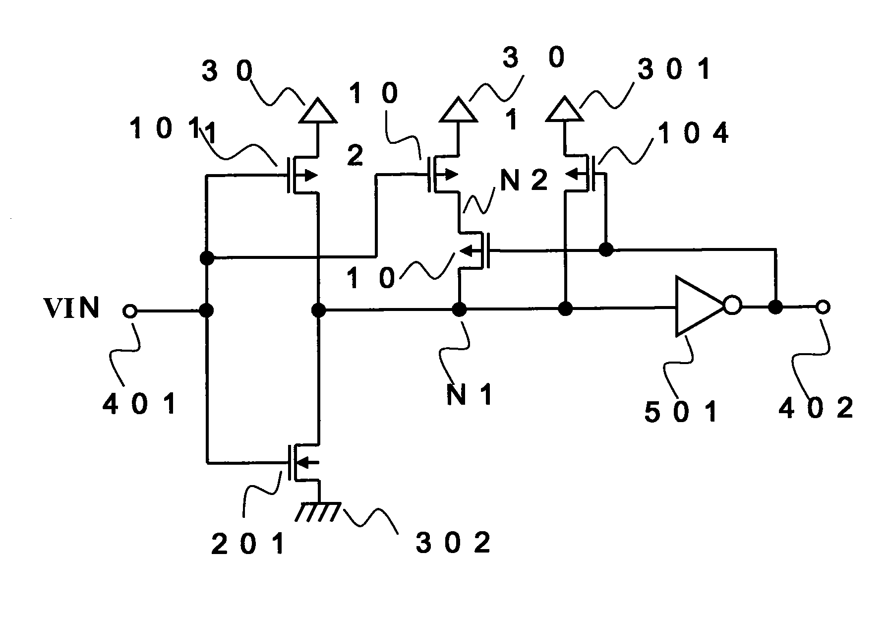
[0034]FIG. 1 is an input circuit having hysteresis characteristics according to a first embodiment of the present invention.

[0035]The input circuit having hysteresis characteristics according to the first embodiment includes PMOS transistors 101 to 104, an NMOS transistor 201, an inverter 501, a first power source 301 (hereinafter referred to as VDD), a second power source 302 (hereinafter referred to as VSS), the voltage of which is lower than that of the first power source 301, an input terminal 401, and an output terminal 402.

[0036]The PMOS transistors 101, 102, and 104 each have a source connected to VDD, while the NMOS transistor 201 has a source connected to VSS. The PMOS transistor 101 and the NMOS transistor 201 each have a gate connected to the input terminal 401 and a drain connected to a node N1. The inverter 501 has an input connected to the node N1 and an output connected to the output terminal 402. The PMOS transistor 102 has a gate connected to the input terminal 401 ...

second embodiment

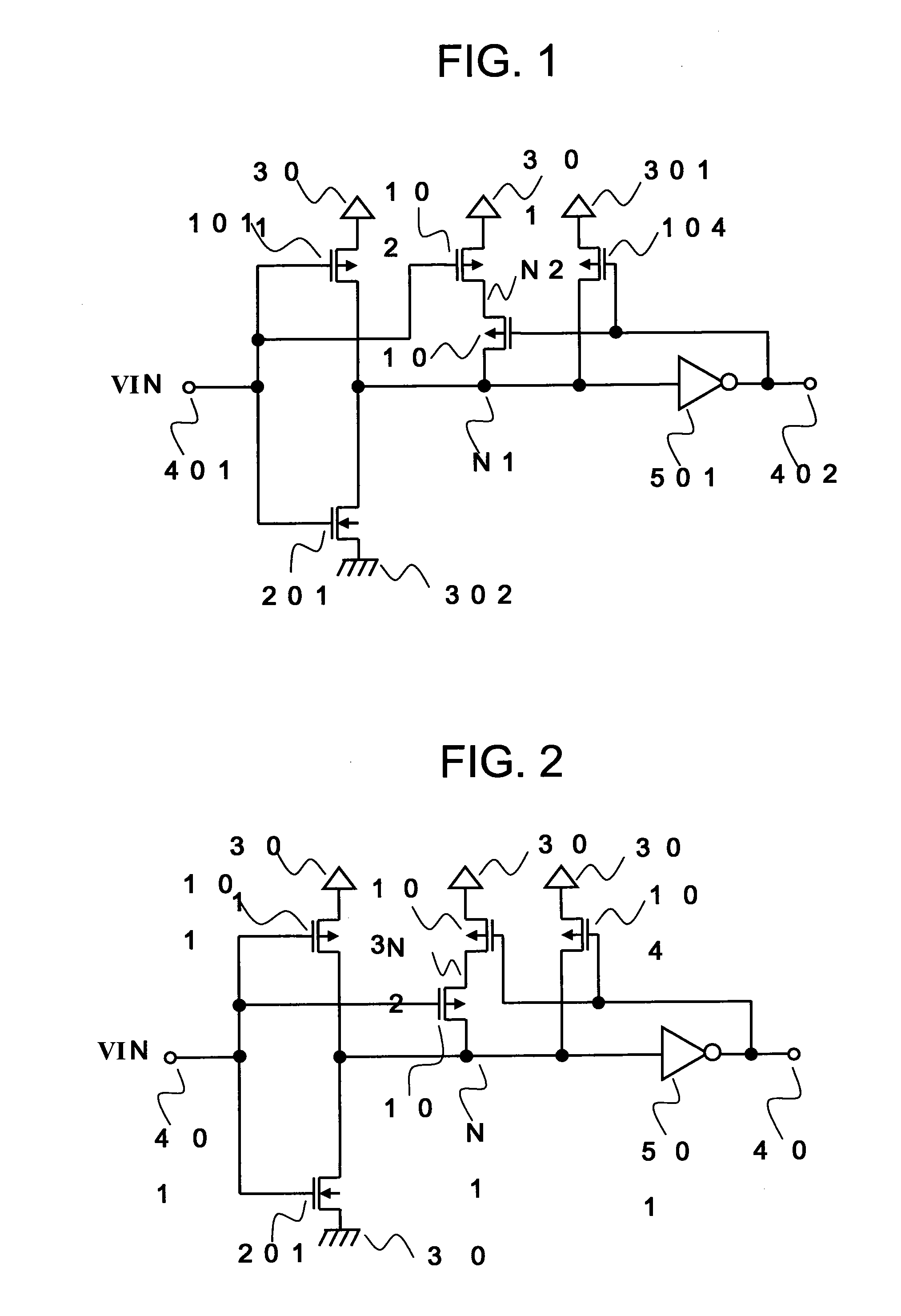
[0045]FIG. 2 is an input circuit having hysteresis characteristics according to a second embodiment of the present invention.

[0046]The input circuit having hysteresis characteristics according to the second embodiment includes PMOS transistors 101 to 104, an NMOS transistor 201, an inverter 501, a first power source 301 (hereinafter referred to as VDD), a second power source 302 (hereinafter referred to as VSS), the voltage of which is lower than that of the first power source 301, an input terminal 401, and an output terminal 402. The second embodiment is different from the first embodiment in the following points. The PMOS transistor 102 has a drain connected to a node N1 and a source connected to a node N2. The PMOS transistor 103 as the interrupting means has a drain connected to the node N2 and a source connected to VDD.

[0047]Next, an operation of the input circuit having hysteresis characteristics according to the second embodiment is described.

[0048]As compared with the first...

third embodiment

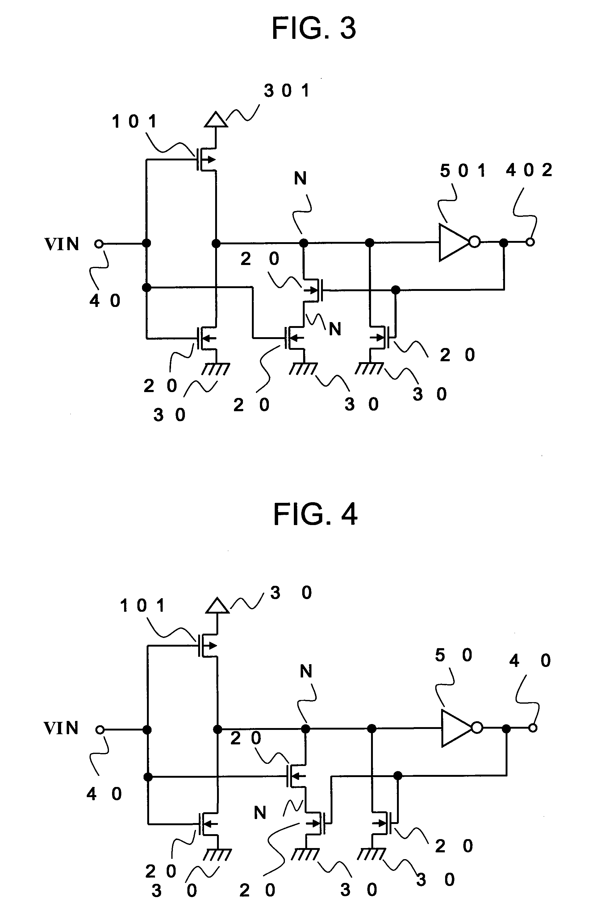
[0050]FIG. 3 is an input circuit having hysteresis characteristics according to a third embodiment of the present invention.

[0051]The input circuit having hysteresis characteristics according to the third embodiment includes NMOS transistors 201 to 204, a PMOS transistor 101, an inverter 501, a first power source 301 (hereinafter referred to as VDD), a second power source 302 (hereinafter referred to as VSS), the voltage of which is lower than that of the first power source 301, an input terminal 401, and an output terminal 402.

[0052]The NMOS transistors 201, 202, and 204 each have a source connected to VSS, while the PMOS transistor 101 has a source connected to VDD. The PMOS transistor 101 and the NMOS transistor 201 each have a gate connected to the input terminal 401 and a drain connected to a node N1. The inverter 501 has an input connected to the node N1 and an output connected to the output terminal 402. The NMOS transistor 202 has a gate connected to the input terminal 401 a...


PUM


Abstract

Provided is an input circuit having hysteresis characteristics that is capable of operating in a wide range of power supply voltage conditions while suppressing power supply voltage dependence of a hysteresis voltage and a response speed. The input circuit is provided with: a circuit for obtaining a small hysteresis voltage under the condition of low power supply voltage (formed of PMOS transistors (101 to 103) and an inverter (501)); and a circuit for obtaining a large hysteresis voltage under the condition of low power supply voltage (formed of PMOS transistors (101 and 104) and the inverter (501)).

Description

RELATED APPLICATIONS[0001]This application claims priority under 35 U.S.C. §119 to Japanese Patent Application No. 2009-258413 filed on Nov. 11, 2009, the entire content of which is hereby incorporated by reference.BACKGROUND OF THE INVENTION[0002]1. Field of the Invention[0003]The present invention relates to an input circuit for a semiconductor integrated circuit, and more particularly, to an input circuit with hysteresis having improved power supply voltage characteristics.[0004]2. Description of the Related Art[0005]A conventional input circuit having hysteresis characteristics is described (see Japanese Patent Application Laid-open No. Hei 10-229331).[0006]FIG. 14 is a circuit diagram illustrating the conventional input circuit with hysteresis. If an input voltage VIN of an input terminal 401 shifts from High to Low, a PMOS transistor 803 for providing hysteresis is turned OFF. Accordingly, a threshold voltage of an inverter circuit is determined by a ratio of ON-state resistan...

Claims


Application Information

Patent Timeline
Patent Type & Authority Applications(United States)
IPC IPC(8): H03K3/00
CPCH03K3/011H03K19/00384H03K3/3565H03K5/1515
Inventor YAMASAKI, TAROUTSUNOMIYA, FUMIYASU
Owner SEIKO INSTR INC
Why Eureka
Try Eureka