Method and device for driving an active matrix display panel

a technology of active matrix and display panel, applied in the field of methods and devices, can solve the problems of reducing the accuracy with which the current level determining the intensity of light emitted by the light-emitting element can be set within the current level

Active Publication Date: 2011-05-12
KONINKLIJKE PHILIPS ELECTRONICS NV
View PDF6 Cites 19 Cited by
  • Summary
  • Abstract
  • Description
  • Claims
  • Application Information

AI Technical Summary

Benefits of technology

It is an object of the invention to provide an active matrix display panel, method of and device for driving such a display panel and display device that allow the current drawn through the light emitting element in a pixel circuit to be set within the time available for each pixel with more accuracy at larger intensity level variations between TOWS.

Problems solved by technology

In particular, large current swings cannot be accurately imposed within the time available for addressing a row.
In addition, it becomes more difficult to match the transistors in the distributed current mirror as they lie further apart, so further decreasing the accuracy with which the current level determining the intensity of light emitted by the light-emitting element can be set within the time available for addressing a row.

Method used


Image

  • Method and device for driving an active matrix display panel
  • Method and device for driving an active matrix display panel
  • Method and device for driving an active matrix display panel

Examples


Embodiment Construction

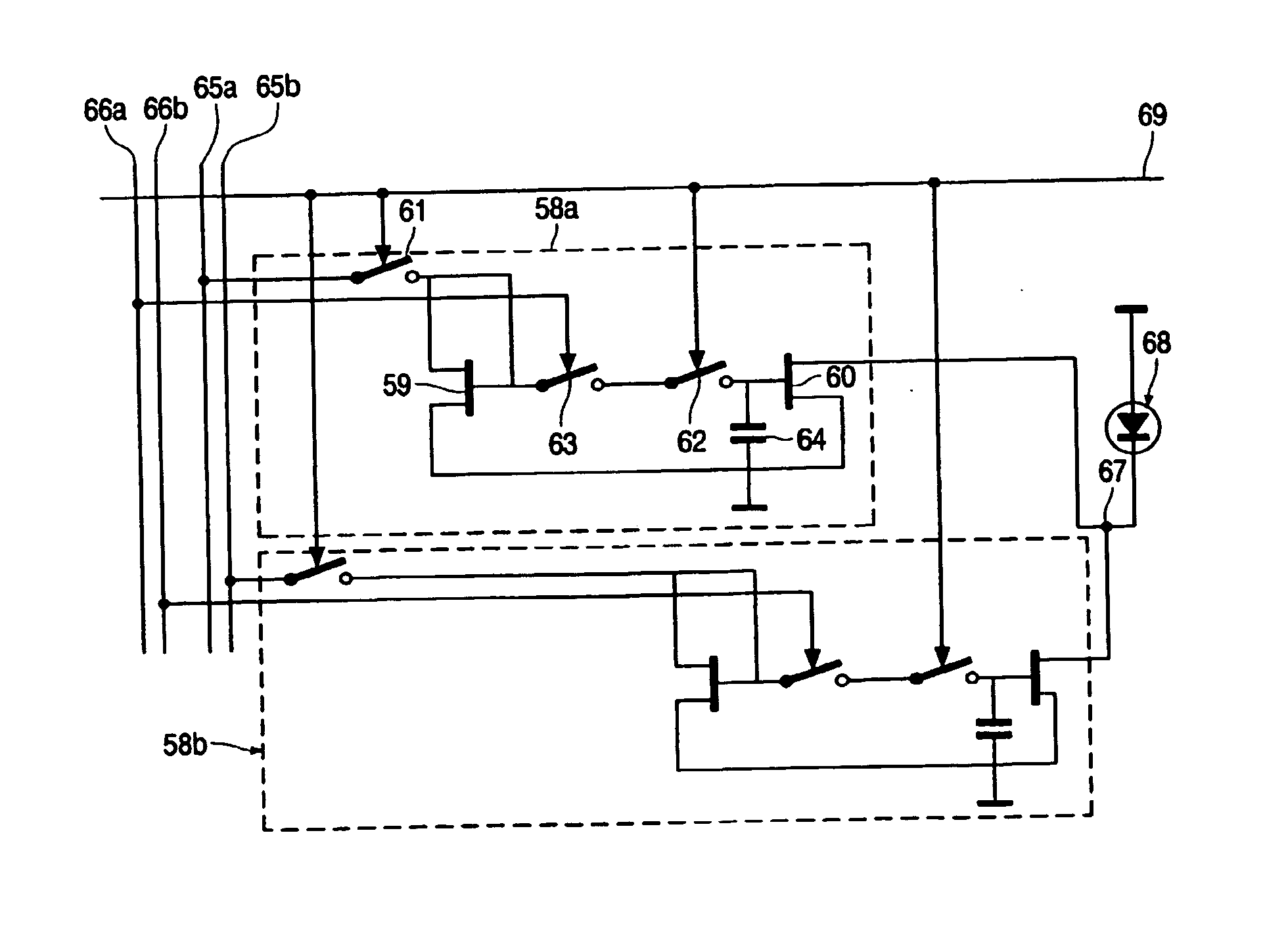
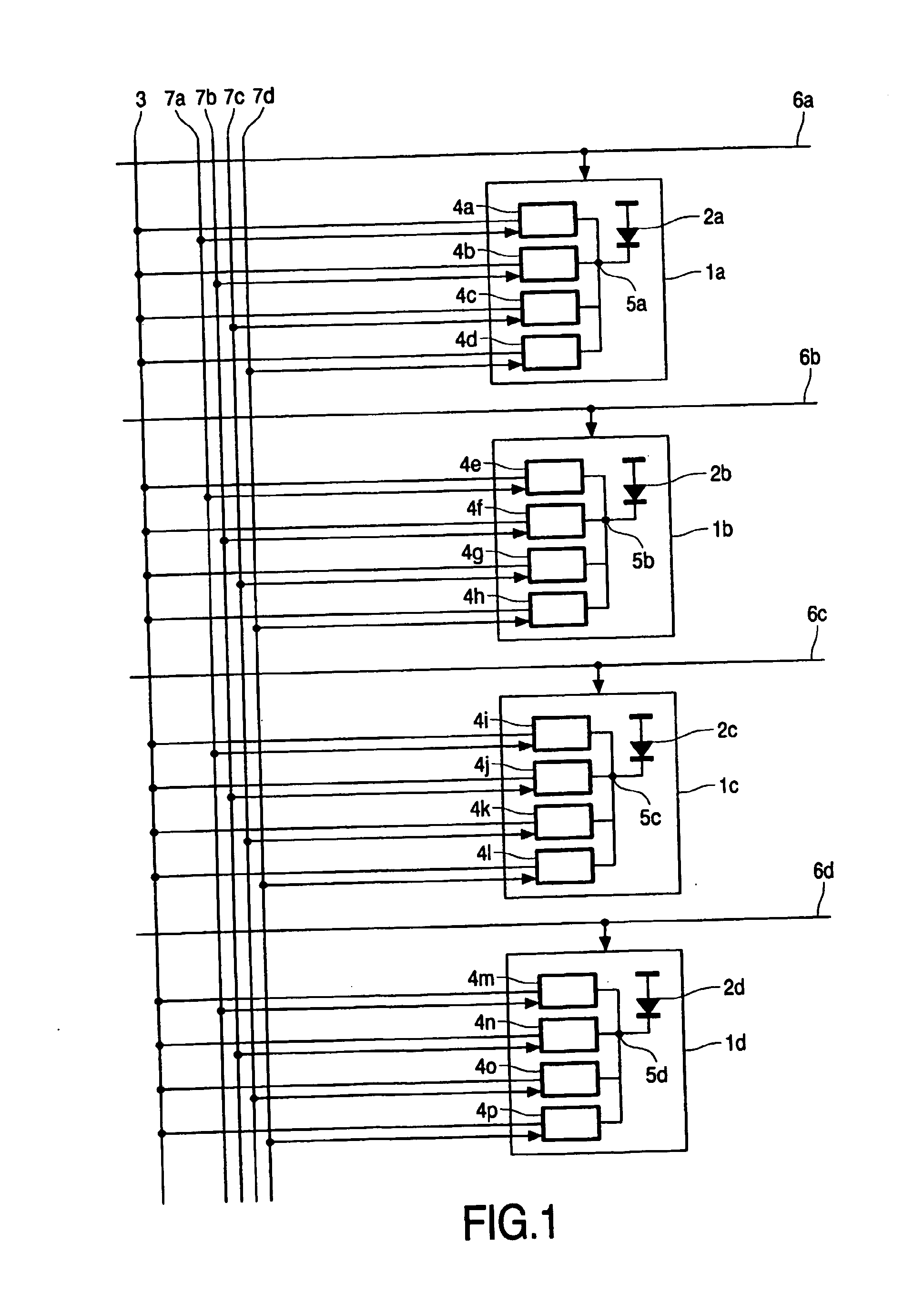
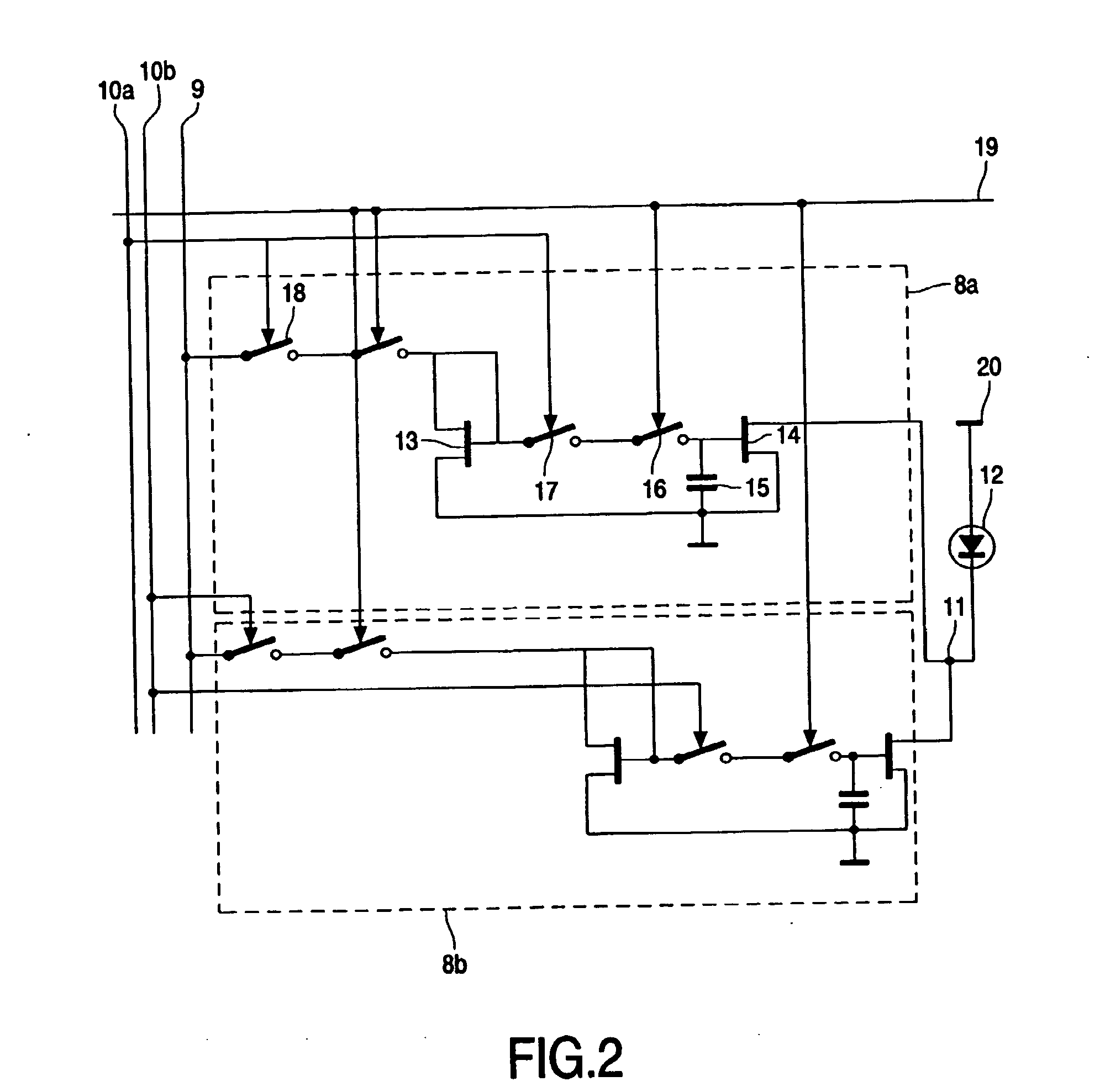
In FIG. 1, a much-simplified section of a column in a first embodiment of an active matrix display panel according to the invention is shown. Four pixel circuits 1a-1d are arranged in a column on a substrate of the active matrix display panel. The substrate may be made of glass or another suitable inorganic material, such as steel, into which the pixel circuits 1a-1d have been formed, for example by etching and / or deposition of material. Alternatively, the substrate may be made of an organic material with suitable optical properties. For simplicity, it will be assumed that each pixel circuit comprises an organic light-emitting diode (OLED) 2a-2d. It is observed that the invention can also be implemented in other types of emissive display panels, in which the intensity of the light emitted by a pixel is determined by the value of a current flowing through a light-emitting element in the pixel. Examples include electro luminescent display panels and Field Emission Display panels. Of c...


PUM


Abstract

An active matrix display panel comprises a substrate, an array of pixel circuits being arranged in a matrix of at least one column and a plurality of rows on the substrate, each pixel circuit comprising a light-emitting element, capable of emitting light of an intensity determined by the value of a current passed through it, and at least one column line, each column line arranged to conduct a reference current, provided by a current driving circuit, when connected to the panel. The pixel circuits in a column are divided into a plurality of groups of at least one pixel circuit. The active matrix display panel comprises at least one current mirror circuit associated with a first group, comprising a first current mirror, arranged to mirror a reference current flowing through a column line to a first current mirror output. Each pixel circuit in the first group comprises at least a first current-memory stage, having an output terminal connected to the light-emitting element, wherein the first current-memory stage is capable of drawing a current determined at least partly by the current mirrored to the first current mirror output through the output terminal. Each current mirror circuit comprises at least one additional current mirror, arranged to mirror a reference current flowing through an associated column line to an additional current mirror output, wherein each additional current mirror output is connected in parallel to the first current mirror output.

Description

FIELD OF THE INVENTIONThe invention relates to an active matrix display panel, comprising a substrate, an array of pixel circuits being arranged in a matrix of at least one column and a plurality of rows on the substrate, each pixel circuit comprising a light-emitting element, capable of emitting light of an intensity determined by the value of a current passed through it, and at least one column line, each column line arranged to conduct a reference current, provided by a current driving circuit, when connected to the panel, wherein the pixel circuits in a column are divided into a plurality of groups of at least one pixel circuit, wherein the active matrix display panel comprises at least one current mirror circuit associated with a first group, comprising a first current mirror, arranged to mirror a reference current flowing through a column line to a first current mirror output, wherein each pixel circuit in the first group comprises at least a first current-memory stage, having...

Claims


Application Information

Patent Timeline
Patent Type & Authority Applications(United States)
IPC IPC(8): G09G5/10G09G3/20G09G3/22G09G3/32
CPCG09G3/2011G09G3/2022G09G3/2077G09G3/22G09G3/3241G09G2300/08G09G2320/0233G09G2300/0814G09G2300/0828G09G2300/0852G09G2310/0251G09G2320/0223G09G2300/0809G09G3/30G09G3/20G09G3/32
Inventor SEMPEL, ADRIANUSHEKSTRA, GERBEN J.FISH, DAVID A.KNAPP, ALAN G.GIRALDO, ANDREAJOHNSON, MARK T.
Owner KONINKLIJKE PHILIPS ELECTRONICS NV
Why Eureka
Try Eureka