

Apparatus for thermal processing with micro-environment
a micro-environment and thermal processing technology, applied in lighting and heating apparatus, electric heating for furnaces, furnaces, etc., can solve the problem of requiring additional wafer handling, and achieve the effect of reducing gas flow
- Summary
- Abstract
- Description
- Claims
- Application Information
AI Technical Summary
Benefits of technology
Problems solved by technology
Method used
Image

Examples
Embodiment Construction
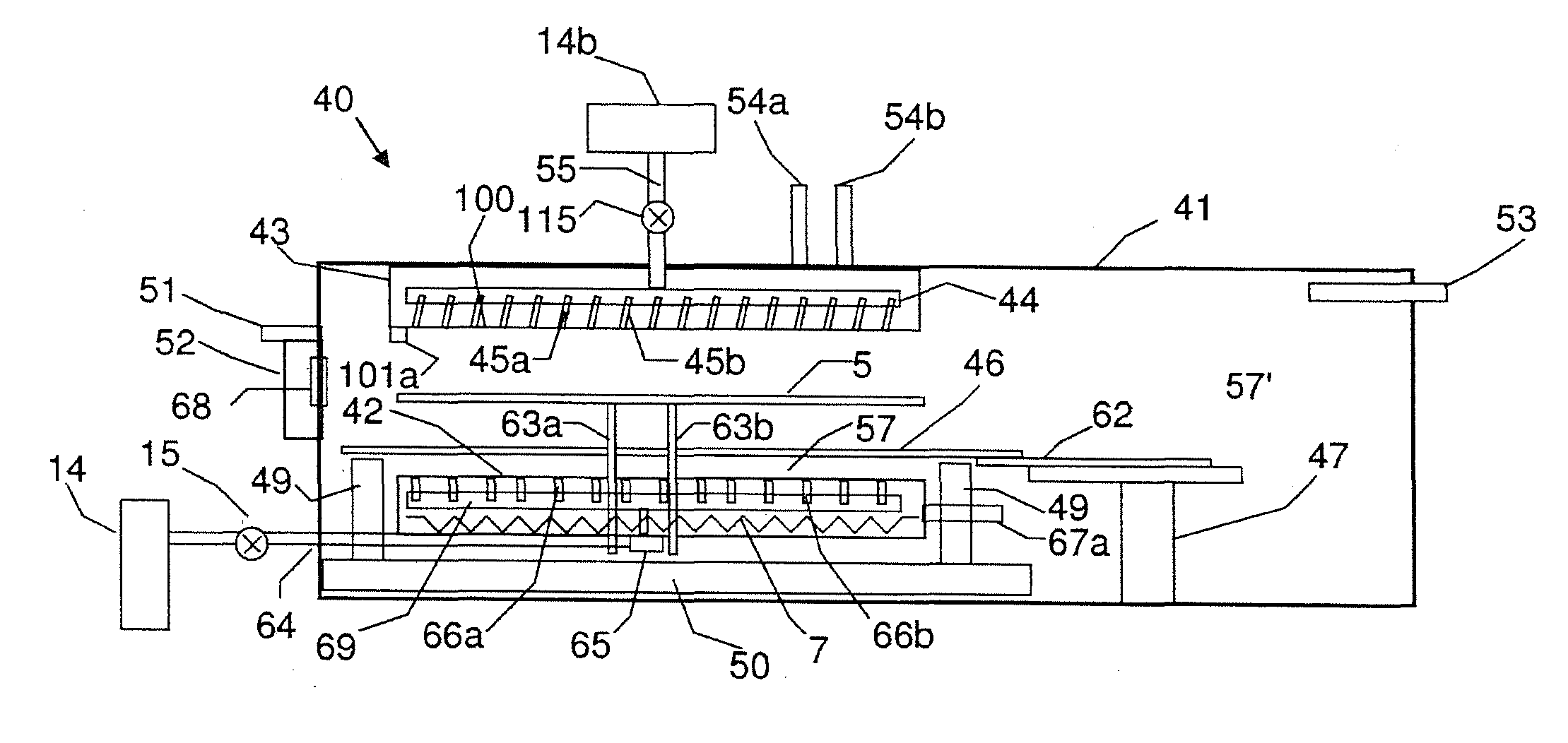
[0002]The disclosed embodiments relate to semiconductor device fabrication, and more particularly to a method and apparatus for processing of semiconductor substrates.
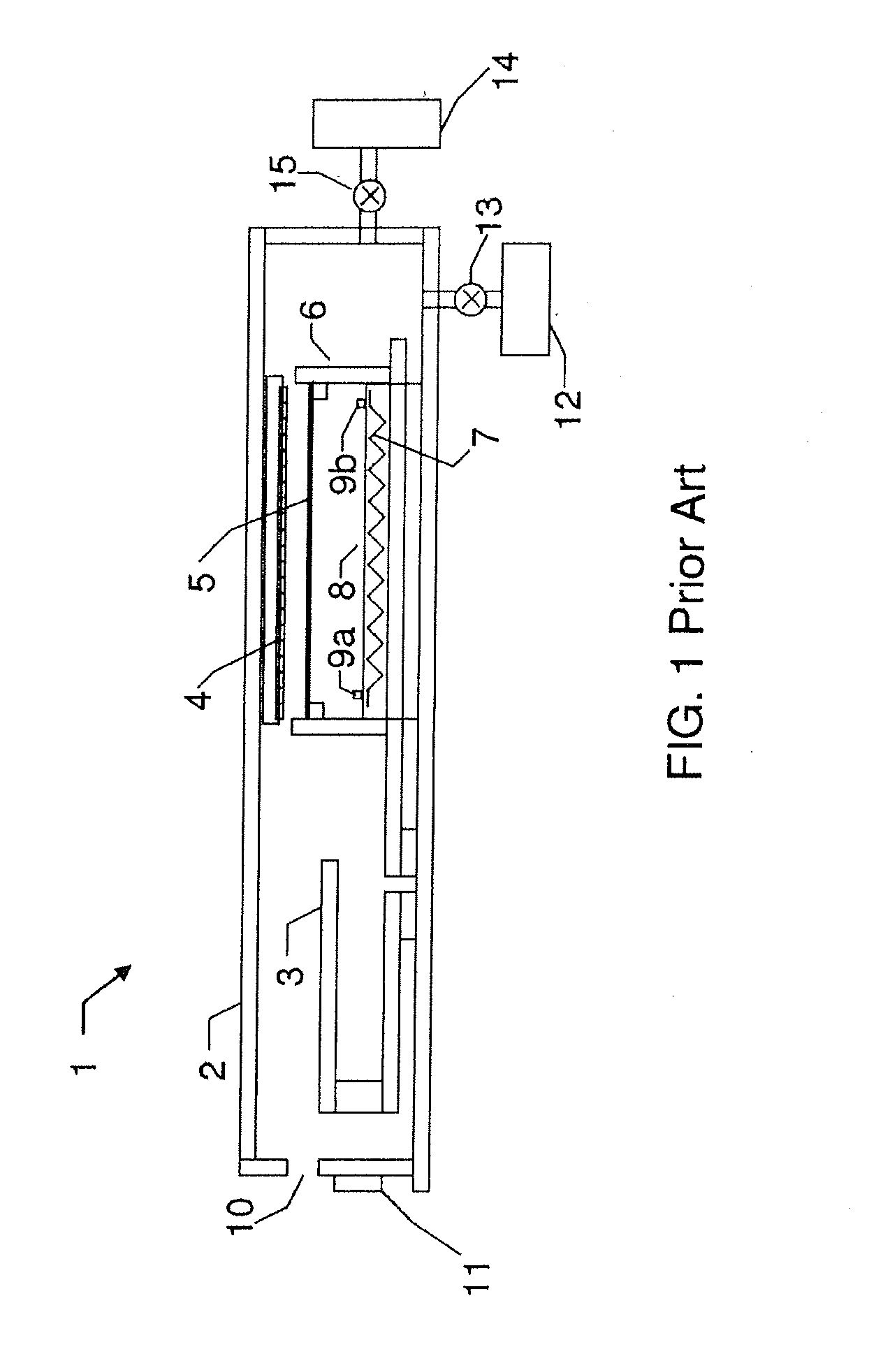
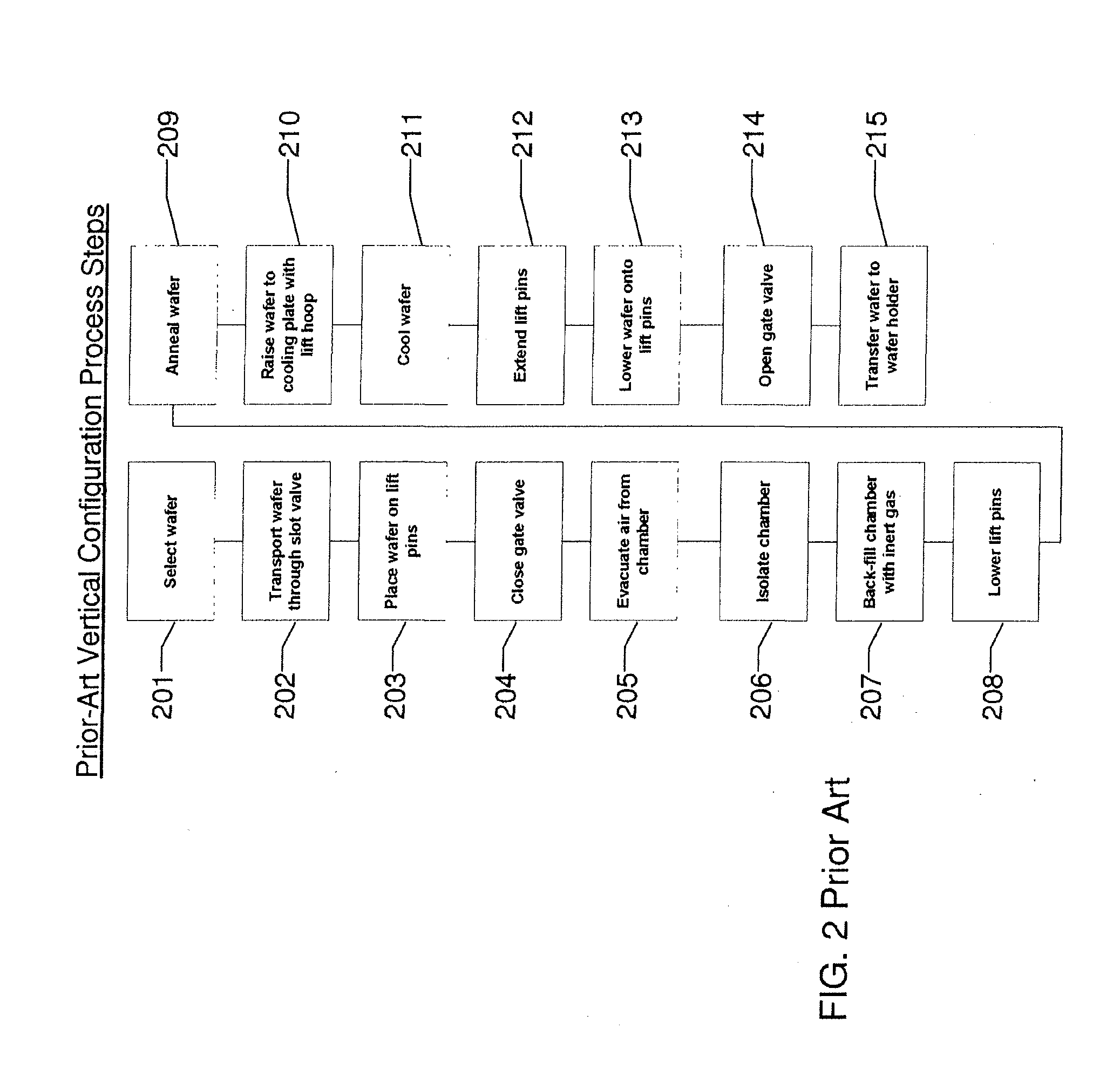
[0003]2. Brief Description of Earlier Developments
[0004]Integrated circuits are generally built on a silicon wafer base and include many components such as transistors, capacitors and other electronic devices connected by multiple layers of wiring, or interconnect. Most advanced chips are now constructed with copper interconnects, since copper has lower resistivity than aluminum. These interconnects are often multi-level and are formed by filling high-aspect ratio features, such as vias and trenches. These features are filled first with dielectric barrier layers followed by metal seed layers using either physical vapor deposition (PVD) or chemical vapor deposition (CVD). After the seed layer, the interconnect features are filled with copper using electrochemical plating (ECP). This process sequence is used for front-en...
PUM
 Abstract
Description
Claims
Application Information