Semiconductor light-emitting device and method for manufacturing the same

a semiconductor and light-emitting device technology, applied in semiconductor devices, lighting apparatus, light and heating equipment, etc., can solve the problems of deterioration of the nitride semiconductor light-emitting device, increase of forward voltage, and increase of electrostatic discharge (esd), so as to improve light-extraction efficiency and improve current distribution

Active Publication Date: 2011-05-19
LG DISPLAY CO LTD
View PDF9 Cites 12 Cited by
  • Summary
  • Abstract
  • Description
  • Claims
  • Application Information

AI Technical Summary

Benefits of technology

[0012]An advantage of the present invention is to provide a semiconductor light-emitting device capable of improving current distribution, and a method for manufacturing the same.
[0013]Another advantage of the present invention is to provide a semiconductor light-emitting device capable of improving light-extraction efficiency, and a method for manufacturing the same.
[0014]Additional advantages and features of the invention will be set forth in part in the description which follows and in part will become apparent to those having ordinary skill in the art upon examination of the following or may be learned from practice of the invention. The objectives and other advantages of the invention may be realized and attained by the structure particularly pointed out in the written description and claims hereof as well as the appended drawings.
[0015]To achieve these and other advantages and in accordance with the purpose of the invention, as embodied and broadly described herein, there is provided a semiconductor light-emitting device comprising: a substrate; an N-type nitride semiconductor layer on the substrate; an active layer on the N-type nitride semiconductor layer; a P-type nitride semiconductor layer on the active layer; a groove in the P-type nitride semiconductor layer to form a predetermined pattern in the P-type nitride semiconductor layer; a light guide of transparent non-conductive material in the groove; and a transparent electrode layer on the P-type nitride semiconductor layer with the light guide.
[0016]In another aspect of the present invention, there is provided a method for manufacturing a semiconductor light-emitting device comprising: forming an N-type nitride semiconductor layer on a substrate; forming an active layer on the N-type nitride semiconductor layer; forming a P-type nitride semiconductor layer on the active layer; forming a groove in the P-type nitride semiconductor layer to form a predetermined pattern in the P-type nitride semiconductor layer; depositing a transparent non-conductive material on an entire area of the P-type nitride semiconductor layer; forming a light guide in the groove by etching the transparent non-conductive material; and forming a transparent electrode layer on the P-type nitride semiconductor layer with the light guide.

Problems solved by technology

This current crowding phenomenon may cause various problems, for example, deterioration of the nitride semiconductor light-emitting device, the increase of forward voltage, and electrostatic discharge (ESD).
In addition, the nitride semiconductor light-emitting device according to the related art has problems such as total reflection of light, and reduction of light extraction efficiency caused by light absorption in the active layer and the electrode.

Method used


Image

  • Semiconductor light-emitting device and method for manufacturing the same
  • Semiconductor light-emitting device and method for manufacturing the same
  • Semiconductor light-emitting device and method for manufacturing the same

Examples


Embodiment Construction

[0033]Reference will now be made in detail to the exemplary embodiments of the present invention, examples of which are illustrated in the accompanying drawings. Wherever possible, the same reference numbers will be used throughout the drawings to refer to the same or like parts.

[0034]Hereinafter, a semiconductor light-emitting device according to the present invention and a method for manufacturing the same will be described with reference to the accompanying drawings.

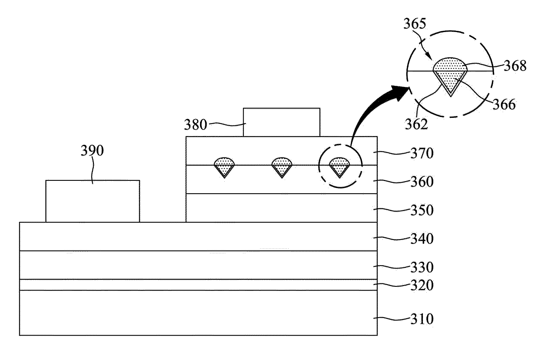
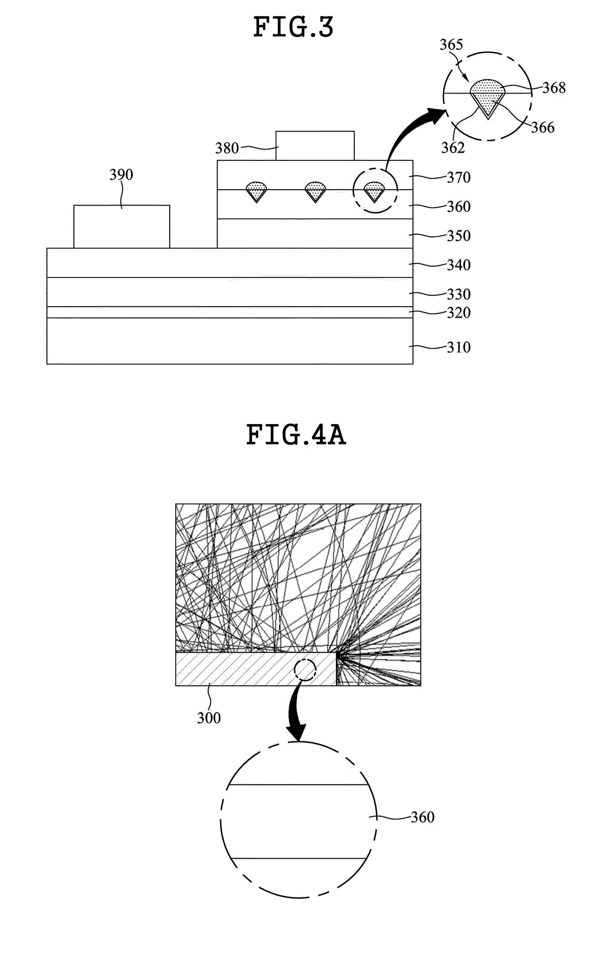
[0035]FIG. 3 is a cross section view illustrating a semiconductor light-emitting device according to one embodiment of the present invention. As shown in FIG. 3, the semiconductor light-emitting device 300 according to one embodiment of the present invention includes a substrate 310, a buffer layer 320, an undoped semiconductor layer 330, an N-type nitride semiconductor layer 340, an active layer 350, a P-type nitride semiconductor layer 360, a light guide 365, a transparent electrode layer 370, a P-type electrode 380...


PUM


Abstract

A semiconductor light-emitting device capable of improving current distribution, and a method for manufacturing the same is disclosed, wherein the semiconductor light-emitting device comprises a substrate; an N-type nitride semiconductor layer on the substrate; an active layer on the N-type nitride semiconductor layer; a P-type nitride semiconductor layer on the active layer; a groove in the P-type nitride semiconductor layer to form a predetermined pattern in the P-type nitride semiconductor layer; a light guide of transparent non-conductive material in the groove; and a transparent electrode layer on the P-type nitride semiconductor layer with the light guide.

Description

CROSS REFERENCE TO RELATED APPLICATIONS[0001]This application claims the benefit of the Korean Patent Application No. 10-2009-0111996 filed on Nov. 19, 2009, which is hereby incorporated by reference as if fully set forth herein.BACKGROUND OF THE INVENTION[0002]1. Field of the Invention[0003]The present invention relates to a semiconductor device, and more particularly, to a nitride semiconductor light-emitting device.[0004]2. Discussion of the Related Art[0005]A nitride semiconductor light-emitting device includes ultraviolet, blue, and green light-emitting regions. Especially, a GaN-based nitride semiconductor light-emitting device can be applied to an optical device of red / green light-emitting diode (LED), and an electronic device corresponding a high-speed switching or high-power device of MESFET (Metal Semiconductor Field Effect Transistor) or HEMT (Hetero Junction Field—Effect Transistor).[0006]FIG. 1 is a cross section view illustrating a nitride semiconductor light-emitting ...

Claims


Application Information

Patent Timeline
Patent Type & Authority Applications(United States)
IPC IPC(8): H01L33/60H01L33/00
CPCH01L33/20H01L33/10
Inventor LEE, UNGPARK, YOON SEOKCHO, WON KEUNJANG, SO YOUNG
Owner LG DISPLAY CO LTD
Why Eureka
Try Eureka