Driving method of switching element and power supply unit

a technology of switching element and power supply unit, which is applied in the direction of electric variable regulation, process and machine control, instruments, etc., can solve the problems of low detection accuracy and high conduction loss of resistor, and achieve the reduction of conduction loss of switching elements, preventing unnecessary waste of driving power, and improving power supply efficiency

Inactive Publication Date: 2011-05-19
RENESAS ELECTRONICS CORP
View PDF7 Cites 7 Cited by
  • Summary
  • Abstract
  • Description
  • Claims
  • Application Information

AI Technical Summary

Benefits of technology

[0025]The unnecessary waste of the driving power can be prevented by driving only one switching element in the light load, and the conduction loss of the switching elements can be reduced by driving a plurality of switching elements in the heavy load. Therefore, the power supply efficiency can be improved over the heavy load from the light load.

Problems solved by technology

However, the Patent Document 2 does not describe the detecting means of the output current.
Although (1) the shunt resistor has high current detection accuracy, it has a problem of high conduction loss generated in the resistor.
Meanwhile, (2) the voltage between a source and a drain of a MOSFET is a method of calculating the drain current by detecting the voltage between a source and a drain of a MOSFET, and although no loss is generated, the method has a problem of low detection accuracy.

Method used


Image

  • Driving method of switching element and power supply unit
  • Driving method of switching element and power supply unit
  • Driving method of switching element and power supply unit

Examples


first embodiment

[0066]The main configuration of a power supply unit according to the first embodiment of the present invention will be described with reference to FIG. 1. FIG. 1 is a block diagram showing the main configuration of the power supply unit according to the first embodiment of the present invention, and it shows only the periphery of a low-side power MOSFET.

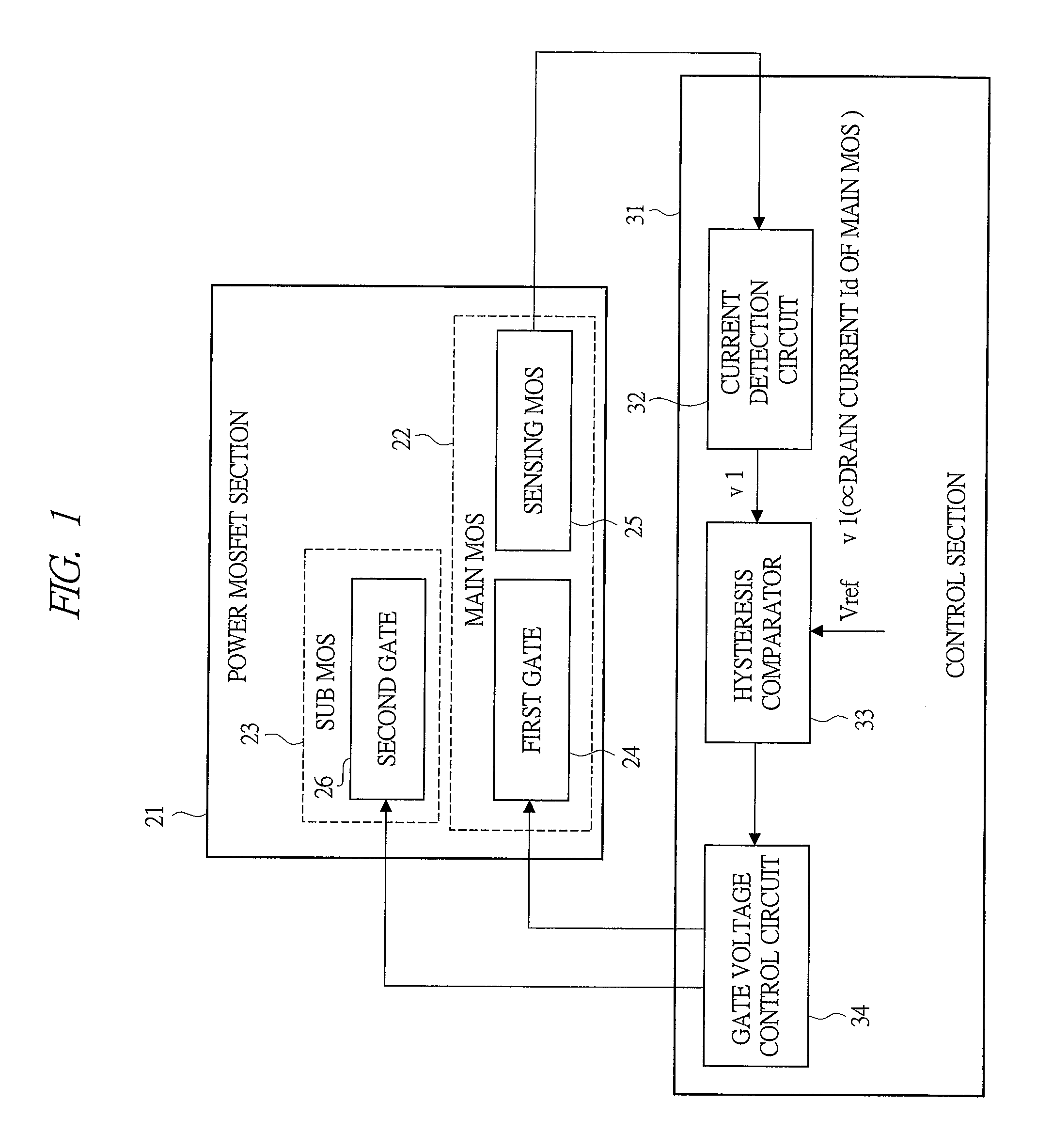
[0067]In FIG. 1, the configuration of the periphery of the low-side power MOSFET of the power supply unit includes a low-side power MOSFET section 21 functioning as a switching element and a control section 31.

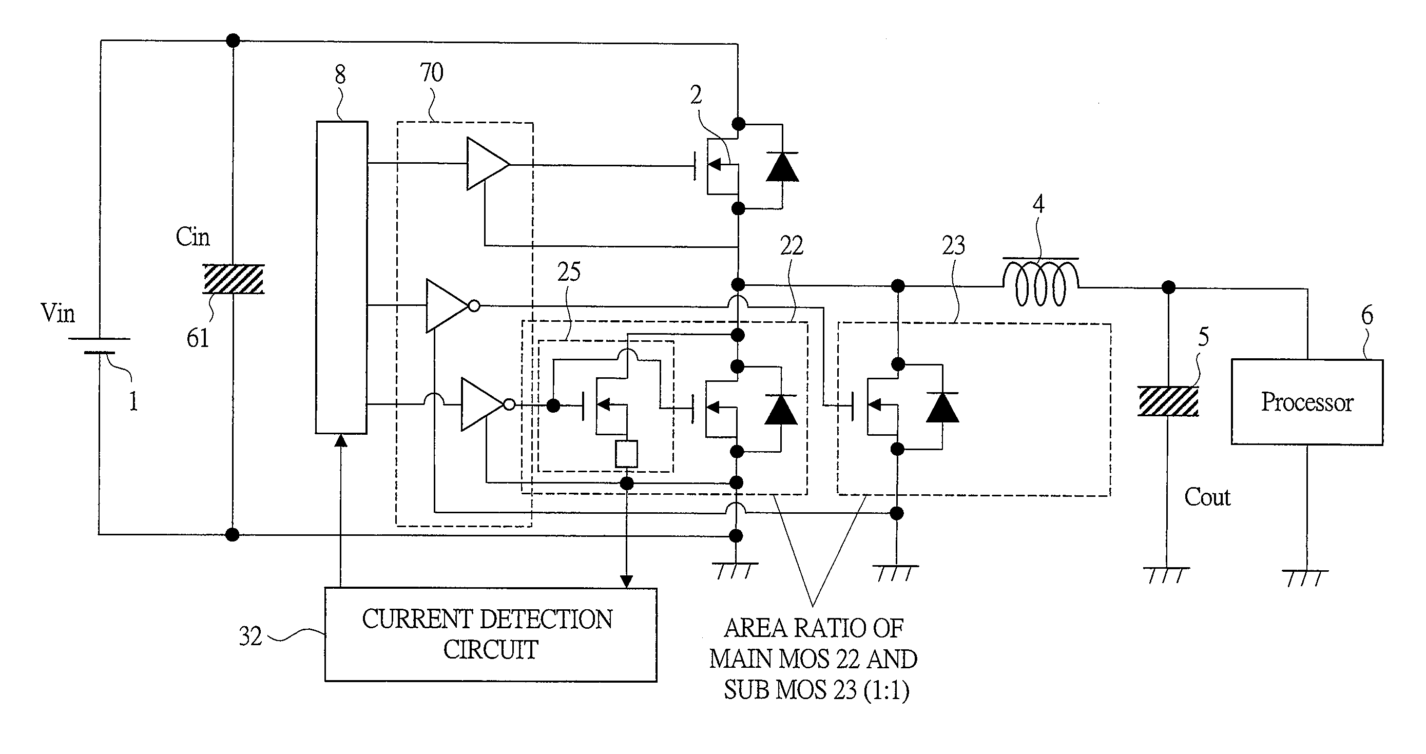
[0068]The power MOSFET section 21 is made up of a main MOS 22 which is always operated and a sub MOS 23 whose operation is stopped in the light load. The main MOS 22 is driven by a first gate 24, the sub MOS 23 is driven by a second gate 26, and a sensing MOS 25 is mounted in only the main MOS 22.

[0069]The control section 31 is made up of a current detection circuit 32, a hysteresis comparator 33 and a gate voltage control circ...

second embodiment

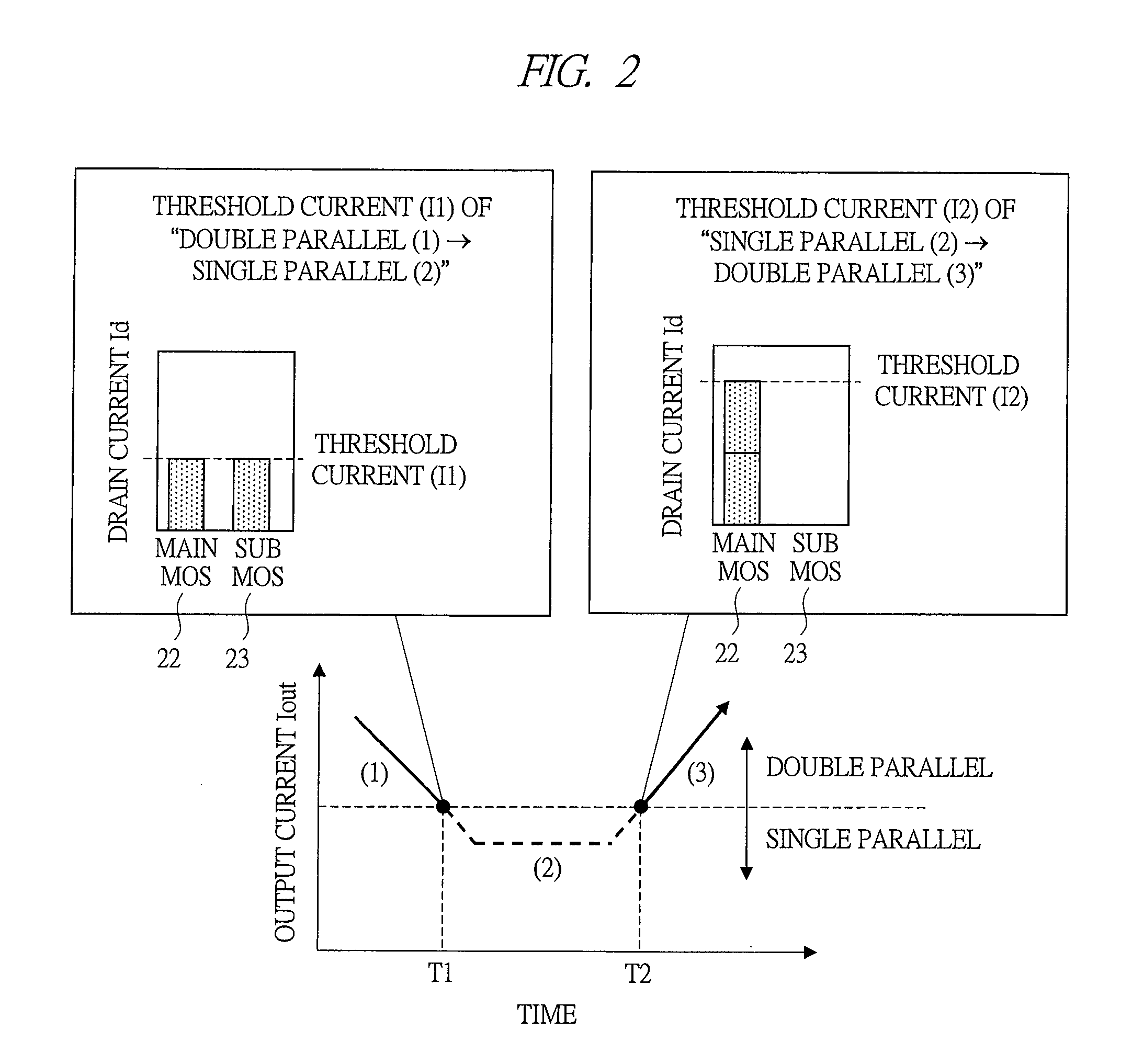
[0094]In the second embodiment, the area ratio of the main MOS 22 and the sub MOS 23 connected in parallel of the low-side power MOSFET in the first embodiment is changed to 1:4.

[0095]The circuit configuration of the power supply unit according to the second embodiment of the present invention will be described with reference to FIG. 7. FIG. 7 is a circuit configuration diagram showing the circuit configuration of the power supply unit according to the second embodiment of the present invention.

[0096]In FIG. 7, the second embodiment is different from the first embodiment shown in FIG. 6 in that the area ratio of the main MOS 22 and the sub MOS 23 connected in parallel of the low-side power MOSFET is 1:4.

[0097]The sum total of the area of the main MOS 22 and the sub MOS 23 is equal to that of the first embodiment shown in FIG. 6. Since the area of the main MOS 22 is reduced, the drive loss is reduced, and the loss when the output current is significantly decreased is reduced.

[0098]Ne...

third embodiment

[0104]In the third embodiment, the two sub MOSs are provided in the configuration of the first embodiment.

[0105]The main configuration of the power supply unit according to the third embodiment of the present invention will be described with reference to FIG. 9. FIG. 9 is a block diagram showing the main configuration of the power supply unit according to the third embodiment of the present invention, and it shows only the periphery of a low-side power MOSFET.

[0106]The third embodiment shown in FIG. 9 is different from the first embodiment shown in FIG. 1 in that a sub MOS 41 which is driven by a third gate 42 and whose operation is stopped in the light load is added, three power MOSFETs are connected in parallel, the two sub MOSs (23, 41) are provided, a first comparator 86 and a second comparator 88 are provided, and reference voltage setting circuits (87, 89) which set the reference voltages Vref of the first comparator 86 and the second comparator 88 are provided. The other conf...


PUM


Abstract

In a power supply unit, a main MOS and a sub MOS connected in parallel in a low-side power MOSFET section, a sensing MOS which is provided on a same semiconductor substrate with the low-side power MOSFET section, detects information corresponding to a load of the low-side power MOSFET section and is smaller in number than the transistors connected in parallel of the low-side power MOSFET section, and a control section for driving the main MOS and the sub MOS based on the information detected by the sensing MOS are provided.

Description

CROSS-REFERENCE TO RELATED APPLICATION[0001]The present application claims priority from Japanese Patent Application No. 2009-262451 filed on Nov. 18, 2009, the content of which is hereby incorporated by reference to this application.TECHNICAL FIELD OF THE INVENTION[0002]The present invention relates to a driving method of a switching element and a power supply unit, and more particularly to downsizing of a chip in a synchronous rectifier circuit used in an electronic device and others.BACKGROUND OF THE INVENTION[0003]The power supply unit shown in FIG. 13 is known as a power supply unit conventionally used in an electronic device and others.[0004]In the power supply unit shown in FIG. 13, the DC power input from a DC input power supply 60 to an input section 51 including an input capacitor 61 is switched in a switching section 52 including an active element 62 based on a control signal output from a driving section 70 of a control section 54, and the power is supplied to a load 66 ...

Claims


Application Information

Patent Timeline
Patent Type & Authority Applications(United States)
IPC IPC(8): G05F1/10
CPCH02M3/1588Y02B70/1466H02M2001/0009Y02B70/10H02M1/0009
Inventor HASHIMOTO, TAKAYUKIMASUNAGA, MASAHIRO
Owner RENESAS ELECTRONICS CORP
Why Eureka
Try Eureka