
Display device and electronic device including the same

a technology of electronic devices and display devices, applied in static indicating devices, electroluminescent light sources, instruments, etc., can solve problems such as less than satisfactory off current, and achieve the effect of suppressing power consumption for displaying still images or the like and further reducing power consumption of display devices

Active Publication Date: 2011-05-19
SEMICON ENERGY LAB CO LTD
View PDF95 Cites 136 Cited by
  • Summary
  • Abstract
  • Description
  • Claims
  • Application Information

AI Technical Summary

Benefits of technology

[0008]One object of one embodiment of the present invention is to provide a display device with reduced power consumption which includes a pixel portion provided with a plurality of pixels having a transistor including an oxide semiconductor.
[0025]According to one embodiment of the present invention, by using a transistor including a high-purity oxide semiconductor in a pixel portion of a display device, off current can be reduced to 1×10⁻¹³ A or lower. Thus, data can be held for a long time and power consumption for displaying a still image or the like can be suppressed.
[0026]Furthermore, the image to be displayed is determined whether it is a still image or a moving image, and in a period in which a still image is displayed, operation of a driver circuit portion is stopped, whereby power consumption of the display device can be further reduced.

Problems solved by technology

However, in a transistor with electric characteristics in such a level, off current is less than satisfactory.

Method used


Image

  • Display device and electronic device including the same
  • Display device and electronic device including the same
  • Display device and electronic device including the same

Examples


embodiment 1

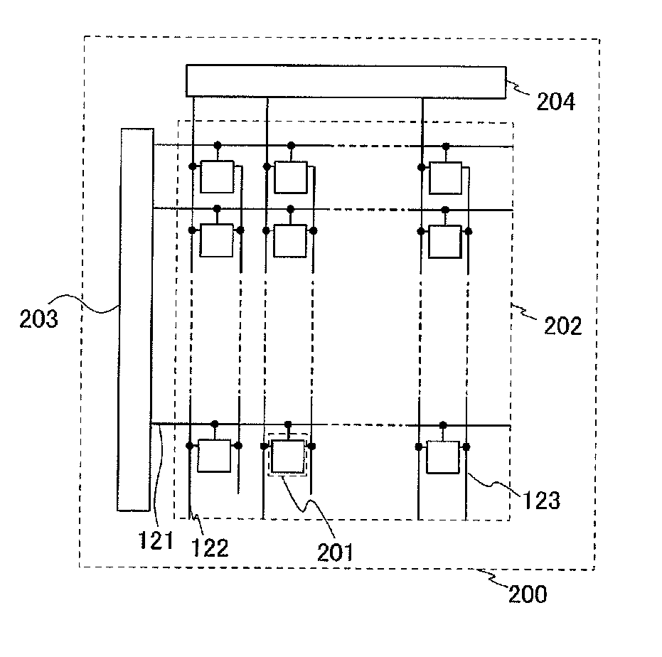
[0057]In this embodiment, an example of a display device which is one embodiment of the present invention will be described. Specifically, a structural example of a pixel in a pixel portion of a display device will be described with reference to FIG. 1, FIG. 2, FIG. 3, FIG. 4, FIGS. 5A to 5C, and FIGS. 6A and 6B.

[0058]FIG. 1 illustrates a structural example of a display device which is one embodiment of the present invention. As is illustrated in FIG. 1, in a display device, a pixel portion 202 in which a plurality of pixels 201 are arranged in a matrix is provided over a substrate 200. In addition, the display device includes a scan line driver circuit 203 and a signal line driver circuit 204 as circuits for driving the plurality of pixels 201. Whether the pixels 201 are in a selected state or in a non-selected state is determined for each row in accordance with a scan signal supplied through the first wiring 121 (a scan line) electrically connected to the scan line driver circuit ...

embodiment 2

[0181]In this embodiment, a structure which leads to a further reduction in power consumption of a display device will be described. Specifically, a structure where power consumption is reduced not only in a pixel portion of a display device, but also in a driver circuit portion of the display device will be described.

[0182]FIG. 7 is a block diagram illustrating an example of a display device. Note that the present invention is not limited to the structure in FIG. 7.

[0183]A display device 1000 in FIG. 7 includes a display panel 1001, a signal generation circuit 1002, a memory circuit 1003, a comparison circuit 1004, a selection circuit 1005, and a display control circuit 1006. The display panel 1001 includes a driver circuit portion 1007 and a pixel portion 1008. The driver circuit portion 1007 includes a gate line driver circuit 1009A and a signal line driver circuit 1009B. The gate line driver circuit 1009A and the signal line driver circuit 1009B have a function to drive the pixe...

embodiment 3

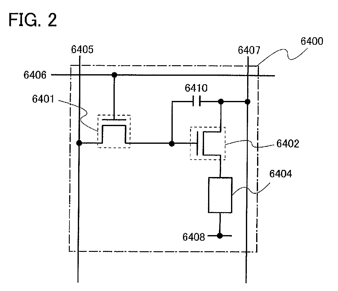
[0245]In this embodiment, a structural example of the first transistor 6401 described in Embodiment 1 and an example of a manufacturing method thereof will be described. In other words, a structural example of a transistor including a high-purity oxide semiconductor and an example of a manufacturing method thereof will be described.

[0246]First, FIGS. 13A and 13B illustrate a planar structure and a cross-sectional structure of an example of a transistor. FIG. 13A is a plan view of a transistor 410 having a top-gate structure and FIG. 13B is a cross-sectional view taken along C1-C2 in FIG. 13A.

[0247]The transistor 410 includes, over a substrate 400, an insulating layer 407, an oxide semiconductor layer 412, a first electrode (one of a source electrode and a drain electrode) 415a, a second electrode (the other of the source electrode and the drain electrode) 415b, a gate insulating layer 402, and a gate electrode 411. A first wiring 414a and a second wiring 414b are provided in contact...


PUM


Abstract

A display device includes a pixel portion including a plurality of pixels each including a first transistor, a second transistor, and a light-emitting element, in which a gate of the first transistor is electrically connected to a scan line, one of a source and a drain of the first transistor is electrically connected to a signal line, and the other of them is electrically connected to a gate of the second transistor; one of a source and a drain of the second transistor is electrically connected to a power supply line and the other of them is electrically connected to the light-emitting element, and the first transistor includes an oxide semiconductor layer. A period when the display device displays a still image includes a period in which output of a signal to all the scan lines in the pixel portion is stopped.

Description

TECHNICAL FIELD[0001]The present invention relates to a display device. Further, the present invention relates to an electronic device including the display device.BACKGROUND ART[0002]In recent years, flat panel displays, which are typified by a liquid crystal display device or an electroluminescence display device (hereinafter, referred to as an EL display device) including an electroluminescence element, are under mass production as the mainstream of the image display device.[0003]In an active matrix liquid crystal display device or in an active matrix EL display device, each pixel in a pixel portion is provided with a transistor. These transistors include a semiconductor layer of silicon (Si) as an active layer.[0004]In contrast, there has been proposed is an image display device in which a transistor includes oxide in its active layer (e.g., see Patent Document 1).REFERENCE[0005][Patent Document 1] Japanese Published Patent Application No. 2006-165528DISCLOSURE OF INVENTION[0006...

Claims


Application Information

Patent Timeline
IPC IPC(8): G09G5/02H01L33/08G09G3/36H05B44/00
CPCH01L27/1225G09G2310/0286G09G3/3233H01L27/3262H10K59/1213H01L29/7869G09G2330/021H10K59/353G09G2300/0842G09G2300/0426G09G2320/0613G09G2300/0439H01L29/78696H01L29/78651H10K59/122H10K59/123G09G3/3266G09G2300/0814G09G2310/08H01L29/78672
Inventor TAKAHASHI, KEIYAMAZAKI, SHUNPEI
Owner SEMICON ENERGY LAB CO LTD
Features
  • Generate Ideas
  • Intellectual Property
  • Life Sciences
  • Materials
  • Tech Scout
  • Unparalleled Data Quality
  • Higher Quality Content
  • 60% Fewer Hallucinations
Learn More