

Solid-state image sensing device
- Summary
- Abstract
- Description
- Claims
- Application Information
AI Technical Summary
Benefits of technology
Problems solved by technology
Method used
Image

Examples
Embodiment Construction
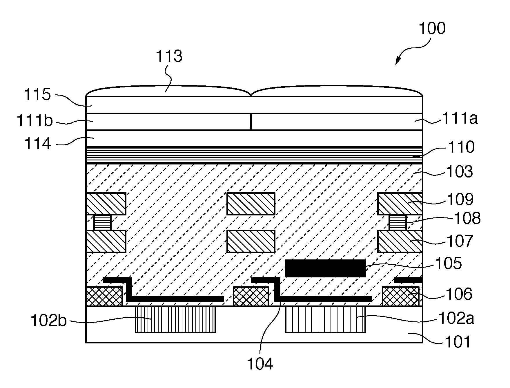
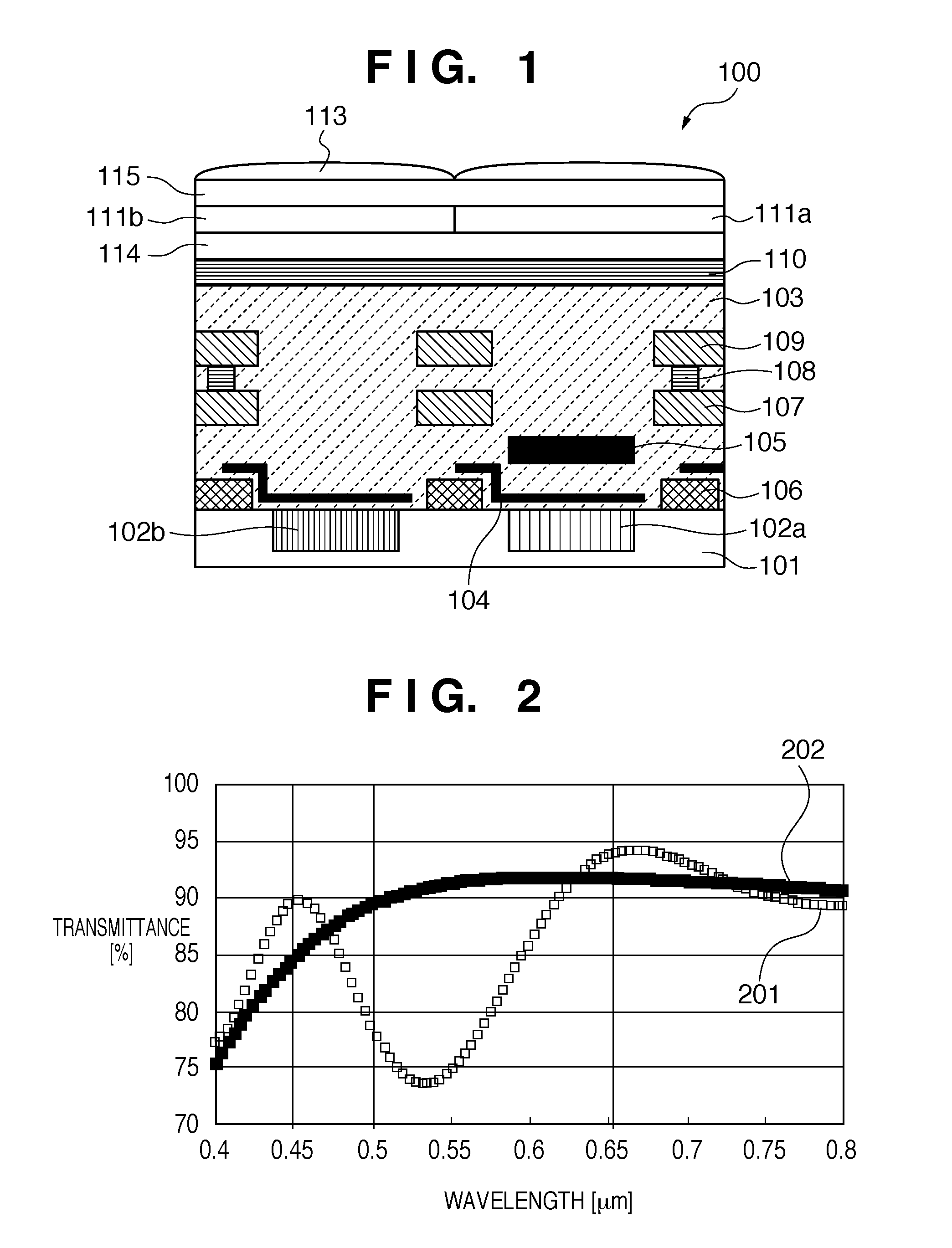
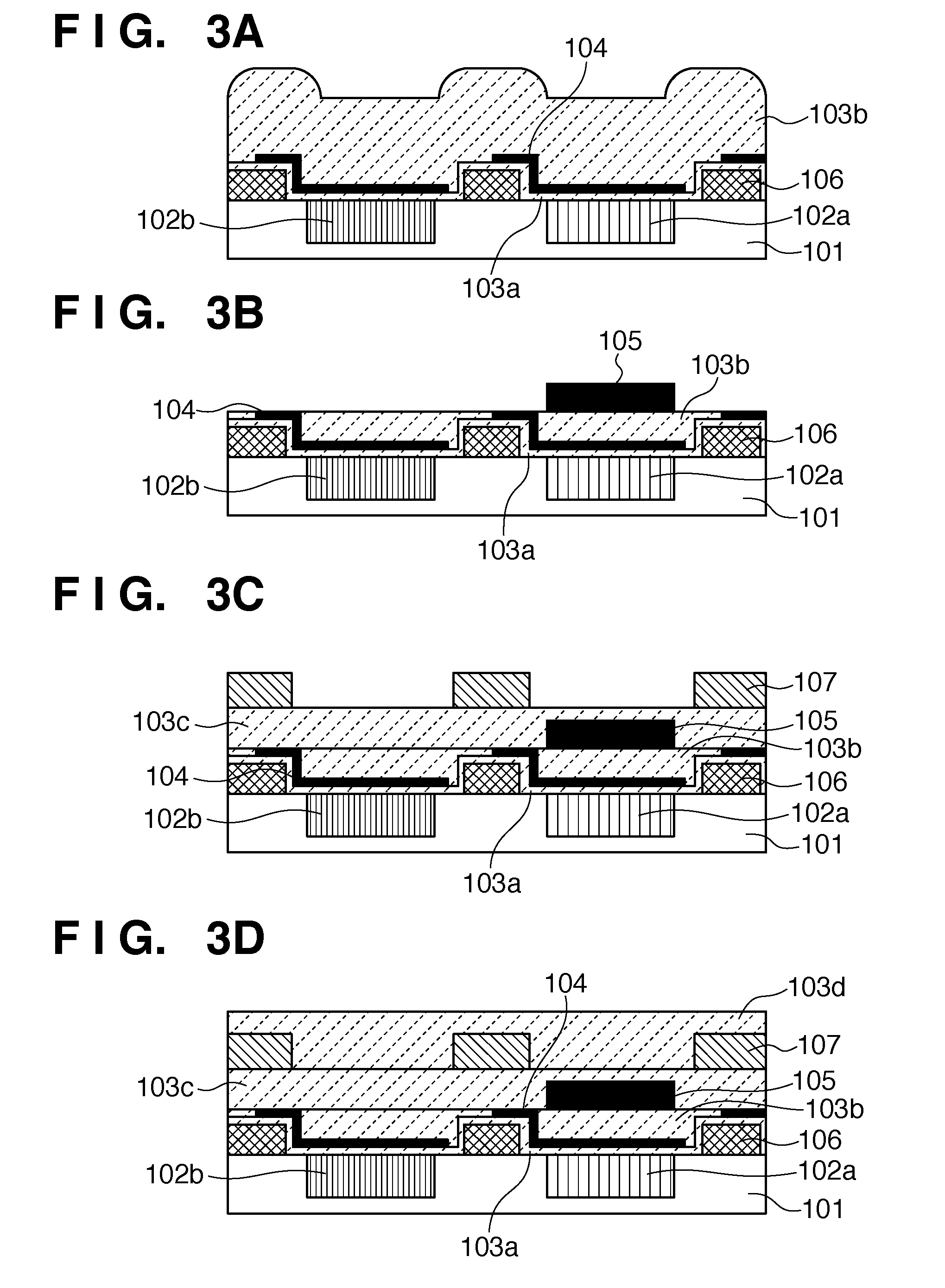
[0013]Preferred embodiments of the present invention will be described below with reference to the accompanying drawings. FIG. 1 is a sectional view showing part of an exemplary solid-state image sensing device 100 according to an embodiment of the present invention. In the solid-state image sensing device 100, light-receiving regions 102a and 102b where incident light is photoelectrically converted are formed in a semiconductor substrate 101 made of silicon or the like. The light-receiving region 102a is for a blue pixel, and the light-receiving region 102b is for a green pixel. A light-receiving region for a red pixel has the same structure as that of the light-receiving region 102a and thus is not shown. The light-receiving region 102a receives the blue component of light entering the solid-state image sensing device 100 through a color filter 111a which transmits blue light. The light-receiving region 102b receives the green component of light entering the solid-state image sens...
PUM
 Abstract
Description
Claims
Application Information