Rectifying antenna device with nanostructure diode

a technology of nanostructure diodes and antenna devices, applied in nanoinformatics, solid-state devices, resonance antennas, etc., can solve the problems of high-speed semiconductor devices, device capacitance, and high cost of construction, and achieve the effect of reducing the cost of construction

Inactive Publication Date: 2011-05-26
RAMOT AT TEL AVIV UNIV LTD
View PDF6 Cites 53 Cited by
  • Summary
  • Abstract
  • Description
  • Claims
  • Application Information

AI Technical Summary

Benefits of technology

[0045]Unless otherwise defined, all technical and/or scientific terms used herein have the same meaning as commonly understood by one of ordinary skill in the art to which the invention pertains. Although methods and materials similar or equivalent to those described herein can be used in the practice

Problems solved by technology

These limitations include the device capacitance and the fragility of high speed semiconductor devices.
Rectennae using large vacuum tubes also have upper frequency limits and are expensive to build.
For example, large arrays of rectennae using conventional vacuum tubes would be prohibitively expensive to build, and could not be produced in a compact form.
As a result, traditional energy ha

Method used


Image

  • Rectifying antenna device with nanostructure diode
  • Rectifying antenna device with nanostructure diode
  • Rectifying antenna device with nanostructure diode

Examples


Embodiment Construction

[0058]The present invention, in some embodiments thereof, relates to a rectifying antenna device and, more particularly, but not exclusively, to a rectifying antenna device operating in the IR and visible light.

[0059]Before explaining at least one embodiment of the invention in detail, it is to be understood that the invention is not necessarily limited in its application to the details of construction and the arrangement of the components and / or methods set forth in the following description and / or illustrated in the drawings and / or the Examples. The invention is capable of other embodiments or of being practiced or carried out in various ways.

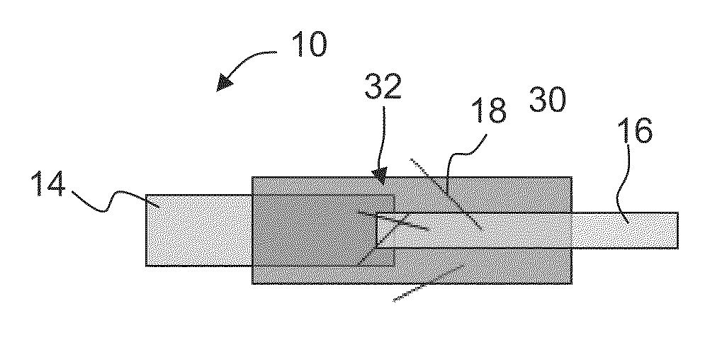
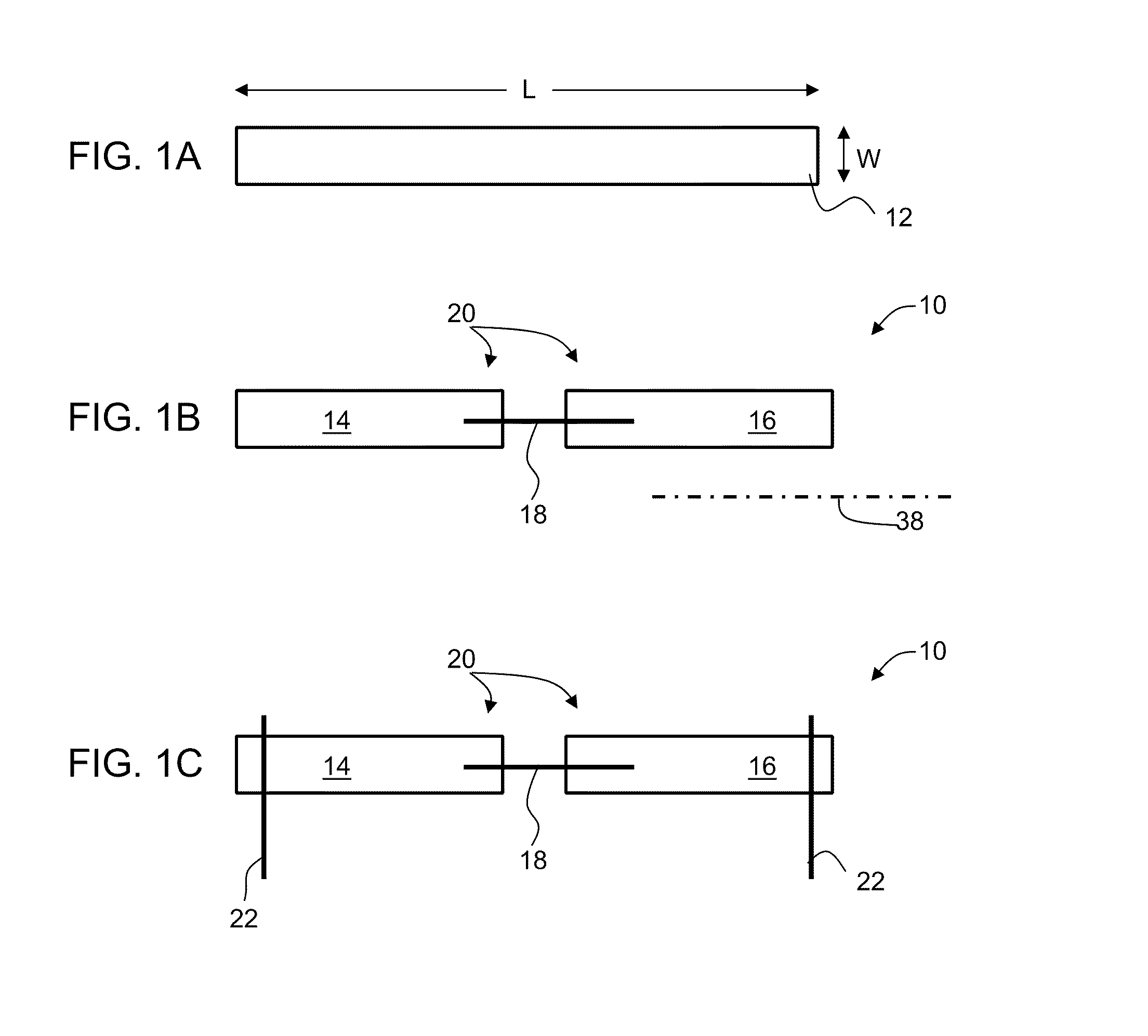
[0060]Referring now to the drawings, FIG. 1A-C illustrate a dipole rectifying antenna device, according to various exemplary embodiments of the present invention. FIG. 1A illustrates a simple dipole antenna 12 having a length L and width W which can be a metallic antenna of nanometric size.

[0061]The term “nanometric size” as used herein refer...


PUM


Abstract

A rectifying antenna device is disclosed. The device comprises a pair of electrode structures, and at least one nanostructure diode contacting at least a first electrode structure of the pair and being at least in proximity to a second electrode structure of the pair. At least one electrode structure of the pair receives AC radiation, and the nanostructure diode(s) at least partially rectifies a current generated by the AC radiation.

Description

FIELD AND BACKGROUND OF THE INVENTION[0001]The present invention, in some embodiments thereof, relates to a rectifying antenna device and, more particularly, but not exclusively, to a rectifying antenna device operating in the infrared (IR) and visible light.[0002]There are many applications in which it is useful to beam energy from an energy production location to a destination at which the energy will be used. The “beamed” energy is typically microwave or radiofrequency. However, many applications for the energy require direct current (DC) power.[0003]A rectifying antenna, also known as a “rectenna” is an electrical device which facilitates the conversion of microwave and radiofrequency alternating current (AC) radiation into DC electrical power. The conversion takes place by a rectifying diode which is incorporated into the antenna. In operation, the antenna gathers electromagnetic energy at a frequency consistent with its size and shape, and the diode rectifies that energy into ...

Claims


Application Information

Patent Timeline
IPC IPC(8): H01L29/06H01L21/329B82Y99/00
CPCB82Y10/00H01L27/28H01L29/0665H01L29/0673H01L29/0676H01L29/1606H02S99/00H01L31/1025H01L51/0048H01L51/0575H01Q1/248H01Q9/28H01Q9/285H01L29/86H01L31/035227Y10S977/742Y10S977/95Y10S977/932H02J50/27H02J50/005Y02E10/50H02J50/001H10K19/00H10K85/221H10K10/20B82Y99/00H01L29/6609H01Q9/16
Inventor HANEIN, YAELBOAG, AMIRSCHEUER, JACOBFRIEDLER, INBAL
Owner RAMOT AT TEL AVIV UNIV LTD
Why Eureka
Try Eureka