Manufacturing method of flexible semiconductor device

Active Publication Date: 2011-05-26
PANASONIC CORP
View PDF3 Cites 11 Cited by
  • Summary
  • Abstract
  • Description
  • Claims
  • Application Information

AI Technical Summary

Benefits of technology

[0021]The present invention uses as a base material, a multilayer film formed by sequentially stacking a first metal layer, an inorganic insulating layer, a semiconductor layer, and a second metal layer. The first metal layer and the second metal layer are processed to form a gate electrode and source/drain electrodes. At the same time, a resin layer is pressure-bonded onto t

Problems solved by technology

Formation of a TFT device made of such a Si material includes a high-temperature process, and thus, a substrate is limited to a material resistant to the process temperature.
Note that a quartz substrate may also be used, but it is expensive and causes cost problems when increasing the s

Method used


Image

  • Manufacturing method of flexible semiconductor device
  • Manufacturing method of flexible semiconductor device
  • Manufacturing method of flexible semiconductor device

Examples


Example

First Embodiment

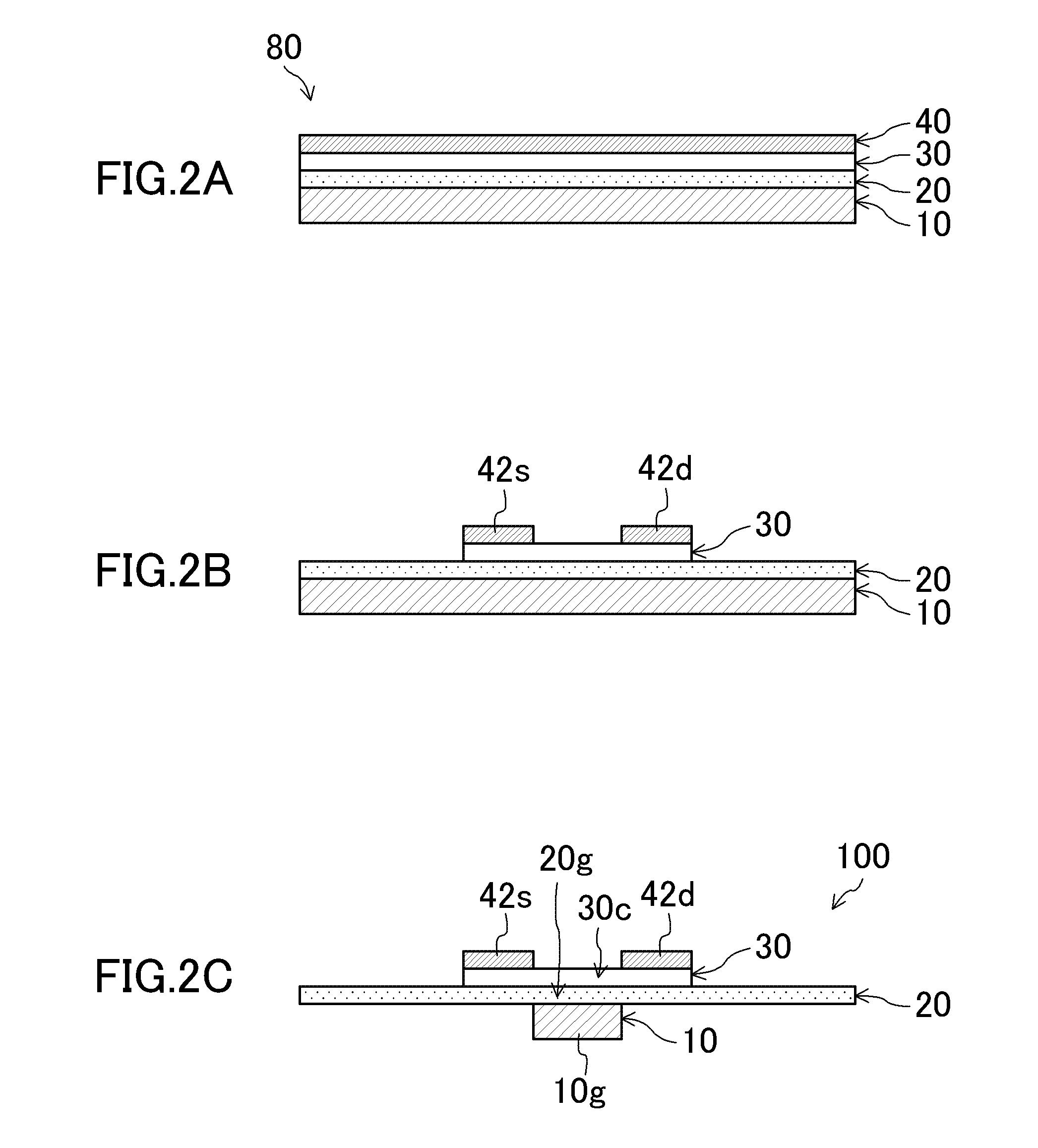
[0051]FIGS. 2 (a)-(d) are cross-sectional views of a manufacturing method of a flexible semiconductor device 100 in the first embodiment of the present invention.

[0052]First, as shown in FIG. 2(a), a multilayer film 80 formed by sequentially stacking a first metal layer 10, an inorganic insulating layer 20, a semiconductor layer 30, and a second metal layer 40, is prepared. The first metal layer 10 and the second metal layer 40 may be made of a same material or different materials. The material of the inorganic insulating layer 20 is not specified, but is preferably a thin film with high dielectric constant, since the inorganic insulating layer functions as a gate insulating film of a thin-film transistor. Furthermore, the material of the semiconductor layer 30 is not specified, but is preferably a thin film with high carrier mobility, since the semiconductor layer 30 functions as a channel of the thin-film transistor. Inorganic semiconductor or organic semiconductor...

Example

Second Embodiment

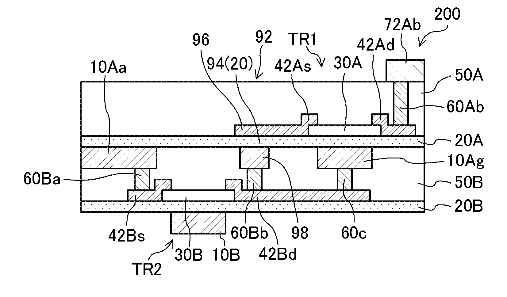
[0095]FIGS. 7(a)-7(d) are cross-sectional views illustrating steps in a manufacturing method of a flexible semiconductor device 110 in a second embodiment of the present invention. This embodiment differs from the first embodiment in that the inorganic insulating layer 20 is provided only under the semiconductor layer 30, the source electrode 42s, and the drain electrode 42d. In the following description, repetitive explanation of the first embodiment is omitted.

[0096]First, as shown in FIG. 7(a), the multilayer film 80 formed by sequentially stacking the first metal layer 10, the inorganic insulating layer 20, the semiconductor layer 30, and the second metal layer 40 is prepared.

[0097]Then, as shown in FIG. 7(b), the source electrode 42s and the drain electrode 42d comprised of the second metal layer 40 is formed by etching the second metal layer 40 in the multilayer film 80. After that, the semiconductor layer 30 and the inorganic insulating layer 20 are removed b...

Example

Third Embodiment

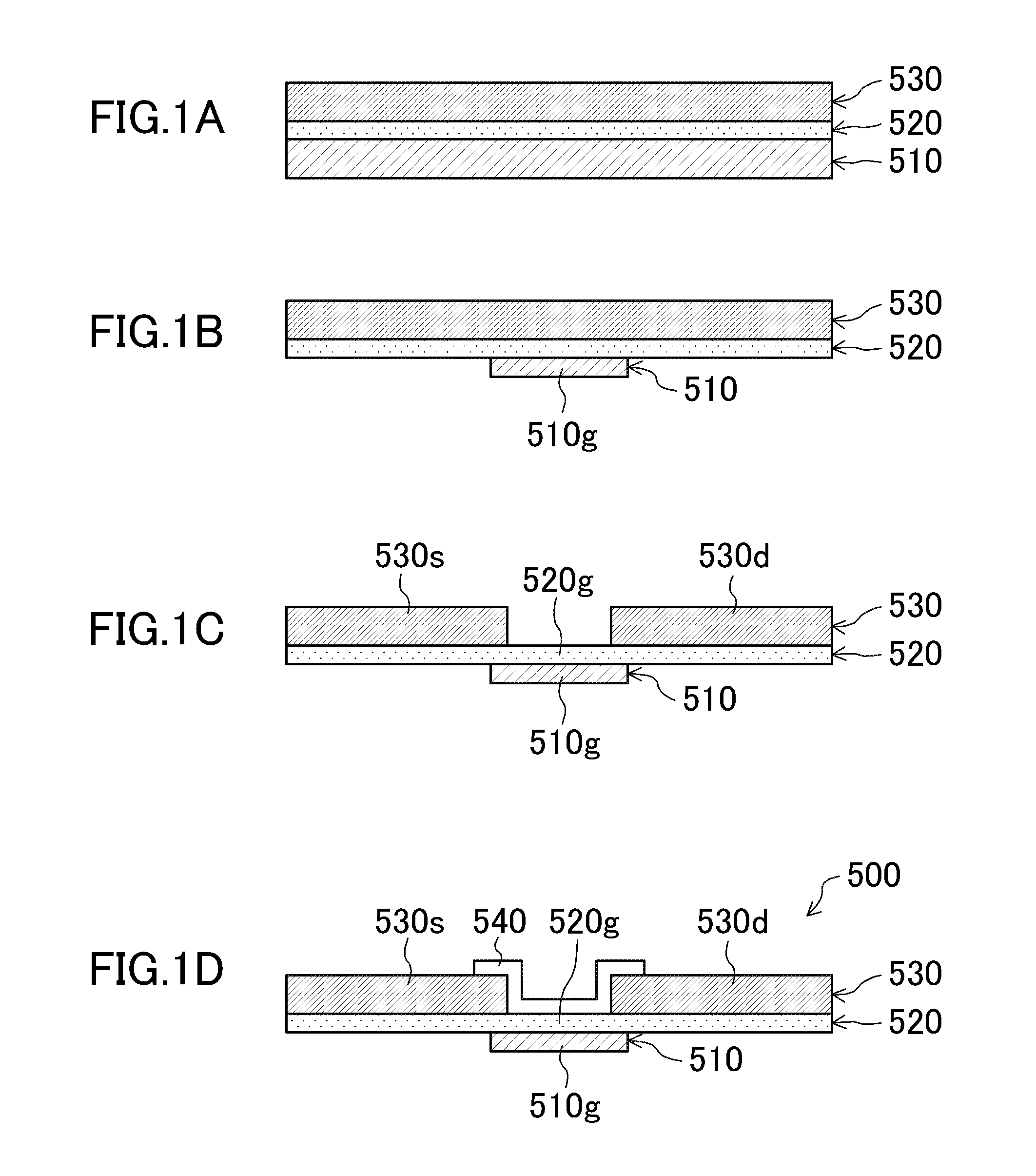
[0103]FIGS. 8(a)-8(e) are cross-sectional views illustrating steps in a manufacturing method of a flexible semiconductor device 120 in a third embodiment of the present invention. This embodiment differs from the first embodiment in that the interlayer connections 60a and 60b connected to the source electrode 42s and the drain electrode 42d, and the interlayer connection 60c connected to the first metal layer 10 are not the paste vias but plated vias. In the following description, repetitive explanation of the first embodiment is omitted.

[0104]First, as shown in FIG. 8(a), the multilayer film 80 formed by sequentially stacking the first metal layer 10, the inorganic insulating layer 20, the semiconductor layer 30, and the second metal layer 40 is prepared.

[0105]Then, as shown in FIG. 8(b), the source electrode 42s and the drain electrode 42d comprised of the second metal layer 40 is formed by etching the second metal layer 40. Furthermore, the semiconductor layer 30 ...


PUM


Abstract

A method includes the steps of preparing a multilayer film 80 formed by sequentially stacking a first metal layer 10, an inorganic insulating layer 20, a semiconductor layer 30, and a second metal layer 40; forming a source electrode 42s and a drain electrode 42d comprised of the second metal layer 40 by etching the second metal layer 40; pressure-bonding a resin layer 50 onto a surface of the multilayer film 80 provided with the source electrode 42s and the drain electrode 42d to burry the source electrode 42s and the drain electrode 42d in the resin layer 50; and forming a gate electrode 10g comprised of the first metal layer 10 by etching the first metal layer 10. The inorganic insulating layer 20g functions as a gate insulating film. The semiconductor layer 30 functions as a channel.

Description

TECHNICAL FIELD[0001]The present disclosure relates to manufacturing methods of flexible semiconductor devices.BACKGROUND ART[0002]With a spread of information terminals, flat panel displays have been increasingly demanded as displays for computers. Furthermore, with the progress of information technology, information which was provided by paper media is increasingly computerized, and electronic paper or digital paper have been increasingly demanded as display media for mobile devices which are thin, lightweight and easily portable (see, e.g., Patent Document 1).[0003]Generally, in a flat panel display, a display medium is formed using a device utilizing liquid crystals, organic electroluminescence (organic EL), electrophoresis, and the like. In such display media, technology with an active matrix device (thin-film transistor (TFT) device) as an image driving element is primarily used to ensure uniformity of screen brightness and a high frame rate. For example, in a conventional com...

Claims


Application Information

Patent Timeline
IPC IPC(8): H01L29/786H01L21/336
CPCH01L27/1266H01L29/458H01L29/4908H01L27/1218H01L29/78681H01L29/7869H01L29/78603H01L2224/24195H01L2224/32245H01L2224/73267H01L2224/82H01L2224/92244H01L2924/3511H01L2924/3512H01L2224/18
Inventor ICHIRYU, TAKASHINAKATANI, SEIICHIHIRANO, KOICHI
Owner PANASONIC CORP
Why Eureka
Try Eureka