Optical semiconductor device having uneven semiconductor layer with non-uniform carrier density

a semiconductor layer and semiconductor technology, applied in the field of optical semiconductor devices, can solve the problems of increasing manufacturing costs, large incident angled light cannot be extracted from the light extracting face, etc., and achieve the effects of improving light output characteristics, increasing current-spreading length of active layers, and reducing drive voltag

Inactive Publication Date: 2011-05-26
STANLEY ELECTRIC CO LTD
View PDF1 Cites 5 Cited by
  • Summary
  • Abstract
  • Description
  • Claims
  • Application Information

AI Technical Summary

Benefits of technology

[0016]According to the presently disclosed subject matter, since currents are supplied even from the side and tip portions of the uneven semiconductor layer, the current-spreading length of the active layer can be increased to improve the light output characteristics. Also, the drive voltage can be decreased. Further, the reliability can be improved by avoiding the breakdown of the semiconductor layers.

Problems solved by technology

Finally, the large-incident-angled light is absorbed by the semiconductor layers, so that the large-incident-angled light cannot be extracted from the light extracting face.
In this case, however, a step for removing the silicon oxide layer 5 is necessary which increases the manufacturing cost.

Method used


Image

  • Optical semiconductor device having uneven semiconductor layer with non-uniform carrier density
  • Optical semiconductor device having uneven semiconductor layer with non-uniform carrier density
  • Optical semiconductor device having uneven semiconductor layer with non-uniform carrier density

Examples


first embodiment

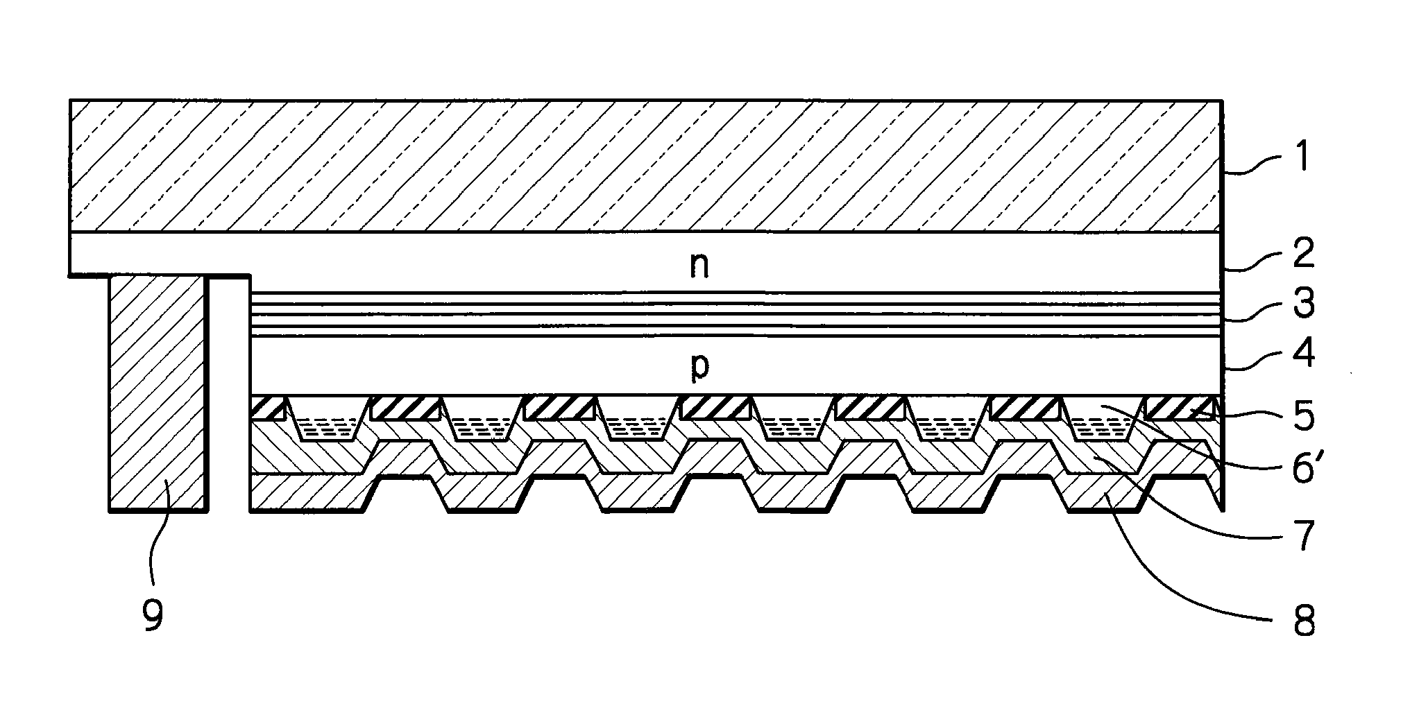
[0029]In FIG. 1, which illustrates the optical semiconductor device according to the presently disclosed subject matter, an uneven trapezoidal-sectional p-type GaN layer 6′ which has a non-uniform carrier density is provided instead of the uneven trapezoidal-sectional p-type GaN layer 6 of FIG. 10 which has a uniform carrier density. In the uneven trapezoidal-sectional p-type GaN layer 6′, the carrier density is higher at the tip portion of one trapezoidal shape than at the bottom portion thereof. In other words, the concentration of p-type impurities is increased stepwise or continuously from the bottom portion of one trapezoidal shape to the tip portion thereof, and accordingly, the carrier density is increased stepwise or continuously from the bottom portion of one trapezoidal shape to the tip portion thereof.

[0030]In order to operate the optical semiconductor device of FIG. 1, a drive voltage is applied between the reflective metal layer (p-side electrode layer) 8, i.e., the tra...

second embodiment

[0082]In FIG. 9, which is a cross-sectional view illustrating the optical semiconductor device according to the presently disclosed subject matter, an upper / lower electrode type (vertical type) optical semiconductor device is illustrated. That is, the growing sapphire substrate 1 of FIG. 1 is removed. Also, a conductive support body 21 having good thermal conductivity is adhered by an adhesive layer 22 to the reflective metal layer 8. Further, an n-side electrode layer 23 instead of the n-side electrode layer 9 of FIG. 1 is provided on the n-type GaN layer 2.

[0083]In order to operate the optical semiconductor device of FIG. 9, in the same way as in the optical semiconductor device of FIG. 1, a drive voltage is applied between the reflective metal layer (p-side electrode layer) 8, i.e., the transparent electrode layer 7 via the conductive support body 21 and the n-side electrode layer 23 to inject currents into the active layer 3. In this case, in the uneven trapezoidal-sectional p-t...


PUM


Abstract

In an optical semiconductor device including a first semiconductor layer of a first conductivity type, an active layer provided on the first semiconductor layer, a second semiconductor layer of a second conductivity type provided on the active layer, an insulating layer provided on a part of the second semiconductor layer, an uneven semiconductor layer of the second conductivity type provided on another part of the second semiconductor layer, and an electrode layer provided on the insulating layer and the uneven semiconductor layer, a density of carriers of the second conductivity type being larger at a tip portion of the uneven semiconductor layer than at a bottom portion of the uneven semiconductor layer.

Description

[0001]This application claims the priority benefit under 35 U.S.C. §119 to Japanese Patent Application No. JP2009-268527 filed on Nov. 26, 2009, which disclosure is hereby incorporated in its entirety by reference.BACKGROUND[0002]1. Field[0003]The presently disclosed subject matter relates to an optical semiconductor device such as alight emitting diode (LED) including III-V group semiconductor compound gallium nitride (GaN).[0004]2. Description of the Related Art[0005]Generally, in an optical semiconductor device including a p-type GaN semiconductor layer, an n-type GaN semiconductor layer and an active semiconductor layer sandwiched by the p-type GaN semiconductor layer and the n-type GaN semiconductor layer, small-incident-angled light emitted from the active semiconductor layer directly or indirectly incident to a light extracting face (upper face) of the semiconductor layers at an incident angle smaller than the critical angle except for its Fresnel component is extracted from ...

Claims


Application Information

Patent Timeline
Patent Type & Authority Applications(United States)
IPC IPC(8): H01L33/20H01L33/32
CPCH01L33/025H01L33/14H01L33/20H01L2933/0016H01L33/387H01L33/405H01L33/42H01L33/32
Inventor MOTEKI, MASAHIKOYOKOBAYASHI, YUSUKE
Owner STANLEY ELECTRIC CO LTD
Why Eureka
Try Eureka