Electrophotographic apparatus
a technology of electrotaxy and apparatus, applied in the direction of electrotaxy, electrotaxy, optics, etc., can solve the problems of surface layer different quantity of wear in the direction of rotational axis, poor image formation and change in quantity of wear
- Summary
- Abstract
- Description
- Claims
- Application Information
AI Technical Summary
Benefits of technology
Problems solved by technology
Method used
Image
Examples
example 1
[0089]First, by means of the plasma-assisted treating apparatus shown in FIG. 6, making use of a high-frequency power source and using an RF band as its frequency, deposited films were formed on a cylindrical substrate (a conductive substrate of 80 mm in diameter, 358 mm in length and 3 mm in wall thickness which was cylindrical and made of aluminum and the surface of which was mirror-finished) to produce an electrophotographic photosensitive member.
[0090]In producing it, in order to form the surface layer the C / (Si+C) of which was to become gradually larger from one end portion toward the other end portion of the electrophotographic photosensitive member, the position of the gas introducing openings 6115 of the source gas introducing pipe 6114 shown in FIG. 6 was adjusted. The position of the gas introducing openings 6115 was adjusted by reducing the number of gas introducing openings 6115 on the end portion side (lower part of the source gas introducing pipe in FIG. 6) where the C...
example 2
[0140]An electrophotographic photosensitive member was so produced that the C / (Si+C) came larger than that in Example 1 when the respective regions in Example 1 were compared with those in this Example, respectively. In its production, the plasma-assisted treating apparatus shown in FIG. 6 the position of the gas introducing openings 6115 of which was adjusted was used to produce the electrophotographic photosensitive member. As film forming conditions, the charge injection blocking layer and the photoconductive layer were formed under the same conditions as those in Example 1 and the surface layer was formed under conditions shown in Table 5 below. As the electrophotographic photosensitive member, two members were produced under the same film forming conditions (layer forming conditions).
TABLE 5ComparativeExampleExample25634Gases & gas flow rates:SiH4 (ml / min) (normal)2626263020H2 (ml / min) (normal)—————B2H6 (ppm based on SiH4)—————NO (ml / min) (normal)—————CH4 (ml / min) (normal)45050...
example 3
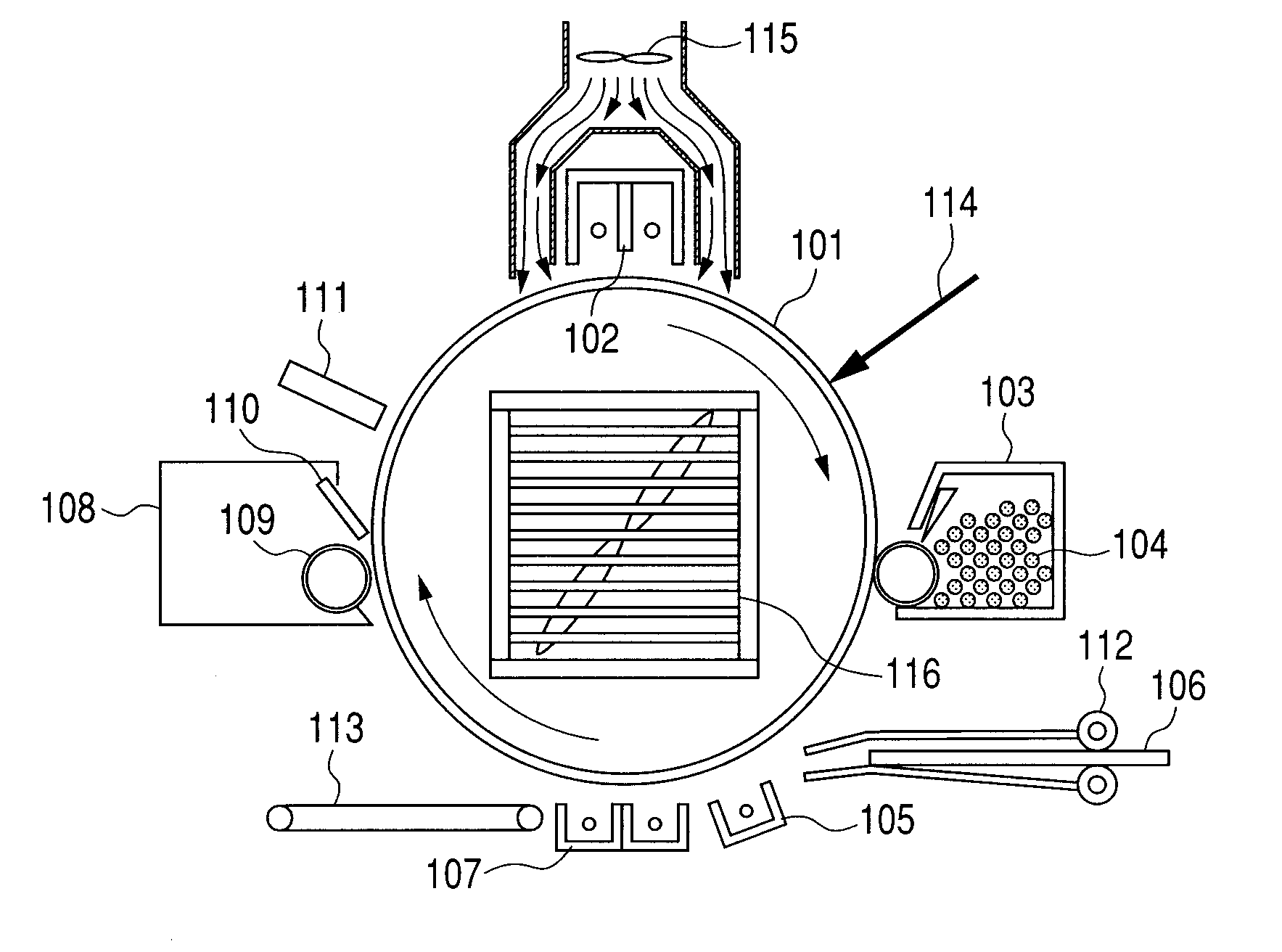
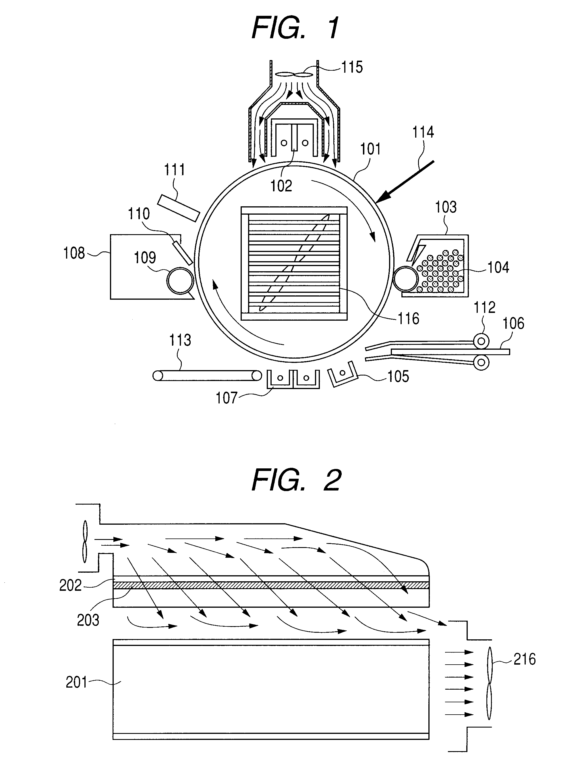
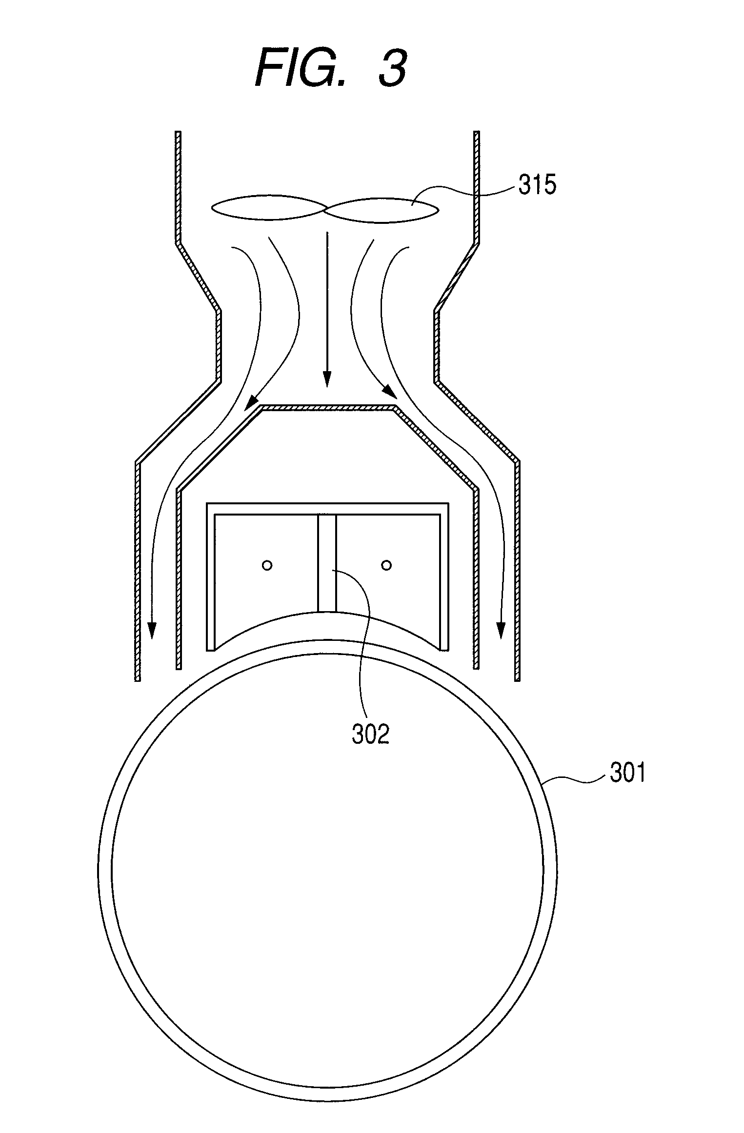
[0163]In Example 3, using an electrophotographic photosensitive member produced under entirely the same conditions as those in Example 1, the wear quantity evaluation and the image evaluation were made in the same way as in Example 1 except that the conversion electrophotographic apparatus used therein was changed for the electrophotographic apparatus shown in FIG. 8. Here, the electrophotographic apparatus shown in FIG. 8 is an apparatus having been so converted that an air current generation means 815 makes the air pass through the inside of a charging member 802 facing the surface of an electrophotographic photosensitive member 801 and thereafter blow over the surface of the electrophotographic photosensitive member 801.
[0164]The results of the wear quantity evaluation and image evaluation are shown in Table 4 above.
[0165]As is clear from the results shown in Table 4, it was seen that the average quantity of wear was reduced by making the air current generation means pass the air...
PUM
| Property | Measurement | Unit |
|---|---|---|
| thickness | aaaaa | aaaaa |
| thickness | aaaaa | aaaaa |
| thickness | aaaaa | aaaaa |
Abstract
Description
Claims
Application Information


