Data transfer device, data transmitting device, data receiving device, and data transfer method

a data transmitting device and data transfer technology, applied in multiplex communication, sustainable buildings, instruments, etc., can solve the problems of power saving, the method of realizing power saving using a sleep mode cannot be applied in limited cases, and the bus cannot be brought into the sleep mod

Inactive Publication Date: 2011-06-02
FUJITSU LTD
View PDF7 Cites 14 Cited by
  • Summary
  • Abstract
  • Description
  • Claims
  • Application Information

AI Technical Summary

Benefits of technology

[0006]On the other hand, the method of changing the transfer mode from the DDR to the SDR can be applied even when a bus is continuously used if the use rate of the bus is low. However, if a signal line for transmitting a signal specifying the transfer mode is provided separately from a signal line for transmitting data signals as in the aforementioned related technology, this causes disadvantageous effects such as complicated configuration of the devices and increase in the cost.
[0008]According to an aspect of an embodiment of the invention, a data transfer device includes a transmitting circuit that transmits data to another data transfer device in a first transfer mode in which data is transferred at every rising and falling of a clock signal or in a second transfer mode in which data is transferred at every rising or at every falling of a clock signal; and a receiving circuit that receives data transmitted from the another data transfer device in the first transfer mode or in the second transfer mode. The transmitting circuit includes a determining unit that determines whether to transmit data in the first transfer mode or in the second transfer mode; a setting unit that sets transfer mode information, which indicates the determined first or second transfer mode, in the data; an output unit that outputs data using the determined first or second transfer mode to the another data transfer device in synchronization with the clock signal; and a transmission control unit that, when a transfer mode determined by the determining unit has changed, instructs the setting unit to set transfer mode information indicating a transfer mode as changed in data and instructs the output unit to output data using the transfer mode as changed after outputting of a first data piece in which a value indicating the transfer mode as changed is set is completed. The receiving circuit includes a receiving unit that receives data transmitted from the another data transfer device in a predetermined one of the first transfer mode and the second transfer mode in synchronization with the clock signal; and a reception control unit that, when transfer mode information contained in the received data is different from the predetermined one of the first data transfer mode and the second data transfer mode, instructs the receiving unit to receive data according to the transfer mode information after receiving the whole of the data containing the transfer mode information.
[0009]The object and advantages of the embodiment will be realized and attained by means of the elements and combinations particularly pointed out in the claims.
[0010]It is to be understood that both the foregoing general description and the following detailed description are exemplary and explanatory and are not restrictive of the embodiment, as claimed.

Problems solved by technology

In recent years, power saving in information processing devices has been an important issue and there has also been a strong demand for power saving in a bus that is a signal transmission path in an information processing device.
However, the method of realizing power saving using a sleep mode can only be applied to limited cases because it is necessary that a bus be not used at all for a certain period.
For example, when a bus is continuously used, the bus cannot be brought into the sleep mode because the data cannot be transferred via the bus in the sleep mode.
However, if a signal line for transmitting a signal specifying the transfer mode is provided separately from a signal line for transmitting data signals as in the aforementioned related technology, this causes disadvantageous effects such as complicated configuration of the devices and increase in the cost.

Method used


Image

  • Data transfer device, data transmitting device, data receiving device, and data transfer method
  • Data transfer device, data transmitting device, data receiving device, and data transfer method
  • Data transfer device, data transmitting device, data receiving device, and data transfer method

Examples


Embodiment Construction

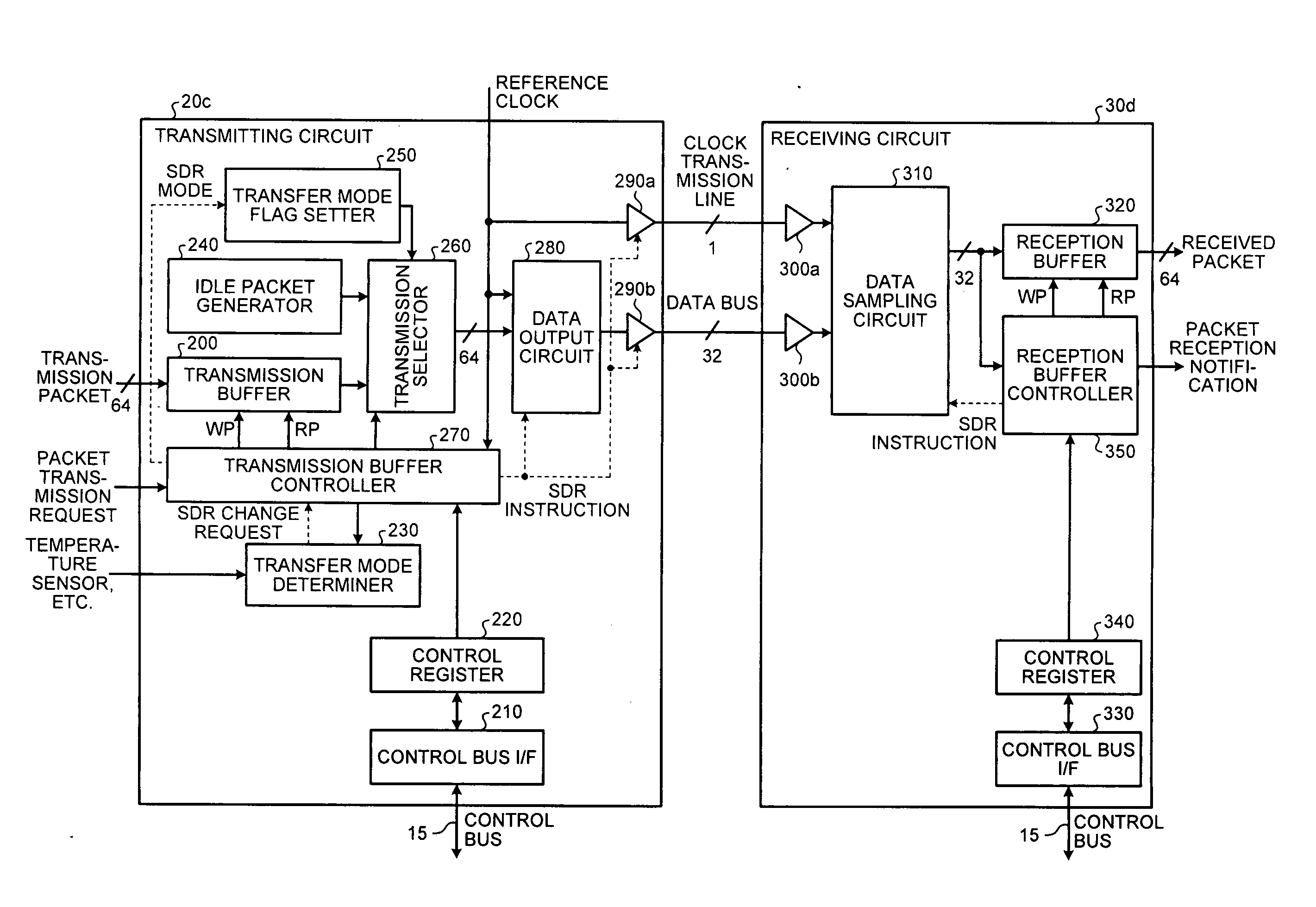
[0034]A preferred embodiment of the present invention will be explained with reference to accompanying drawings. It should be noted that the invention is not limited to the embodiment. In the embodiment described below, an example in which the data transfer device disclosed herein is separated into two independent circuits, which are a transmitting circuit and a receiving circuit. However, the data transfer device may be configured as one circuit having both the configurations of the transmitting circuit and the receiving circuit.

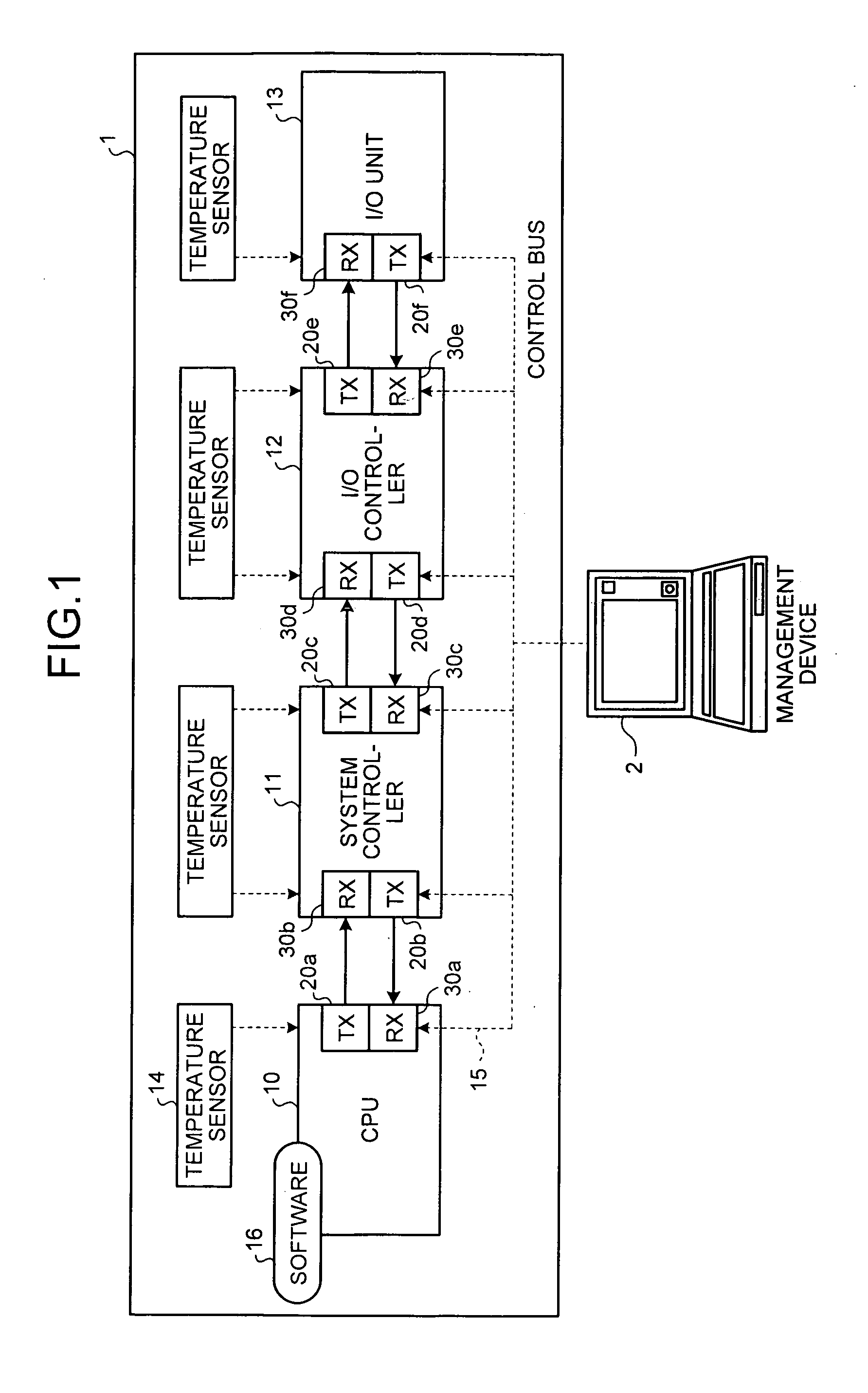
[0035]First, an information processing device including the transmitting circuit and the receiving circuit according to the embodiment will be described. FIG. 1 is a block diagram illustrating a configuration of an information processing device 1 including the transmitting circuit and the receiving circuit according to the embodiment. As illustrated in FIG. 1, the information processing device 1 includes a central processing unit (CPU) 10, a system controll...


PUM


Abstract

The change of the transfer mode is notified using a predetermined bit in a header of a packet. Accordingly, the transfer mode can be dynamically switched from a DDR to a SDR, in which power consumption is low, without complicating the configuration. When the transfer mode is the SDR, further power saving is realized by changing the slew rate or stopping some circuits.

Description

CROSS-REFERENCE TO RELATED APPLICATION[0001]This application is a continuation of International Application No. PCT / JP2008 / 063770, filed on Jul. 31, 2008, the entire contents of which are incorporated herein by reference.FIELD[0002]The embodiment discussed herein is directed to a data transfer device, a data transmitting device, a data receiving device and a data transfer method.BACKGROUND[0003]In recent years, power saving in information processing devices has been an important issue and there has also been a strong demand for power saving in a bus that is a signal transmission path in an information processing device. As one attempt to realize power saving of a bus, the PCI Express, which is an I / O bus widely used at present, has a mode called a sleep mode. The sleep mode is a mode in which a bus is brought into a stopped state in such a case where the bus has not been used for a certain period.[0004]As another attempt to reduce power consumption in a bus, changing the transfer mo...

Claims


Application Information

Patent Timeline
Patent Type & Authority Applications(United States)
IPC IPC(8): H04J3/00
CPCG06F13/4239Y02B60/1235Y02B60/1228Y02D10/00
Inventor SUZUKI, KENJI
Owner FUJITSU LTD
Why Eureka
Try Eureka