Electron microscope

a technology of electron microscope and electron microscope, which is applied in the field of electron microscope, can solve the problem that the observed image cannot be interpreted, and achieve the effect of high resolution of the ptem image and versatile use of i

Inactive Publication Date: 2011-06-09
HITACHI HIGH-TECH CORP
View PDF11 Cites 27 Cited by
  • Summary
  • Abstract
  • Description
  • Claims
  • Application Information

AI Technical Summary

Benefits of technology

According to the present invention, it is possible to make higher the resolution of a PTEM image, to thereby realize a versatile use thereof.

Problems solved by technology

However, an image which can be observed using the transmission electron microscope is an image formed by the interference between electron beams, and hence the observed image cannot be interpreted as it is.

Method used


Image

  • Electron microscope
  • Electron microscope
  • Electron microscope

Examples


embodiment 1

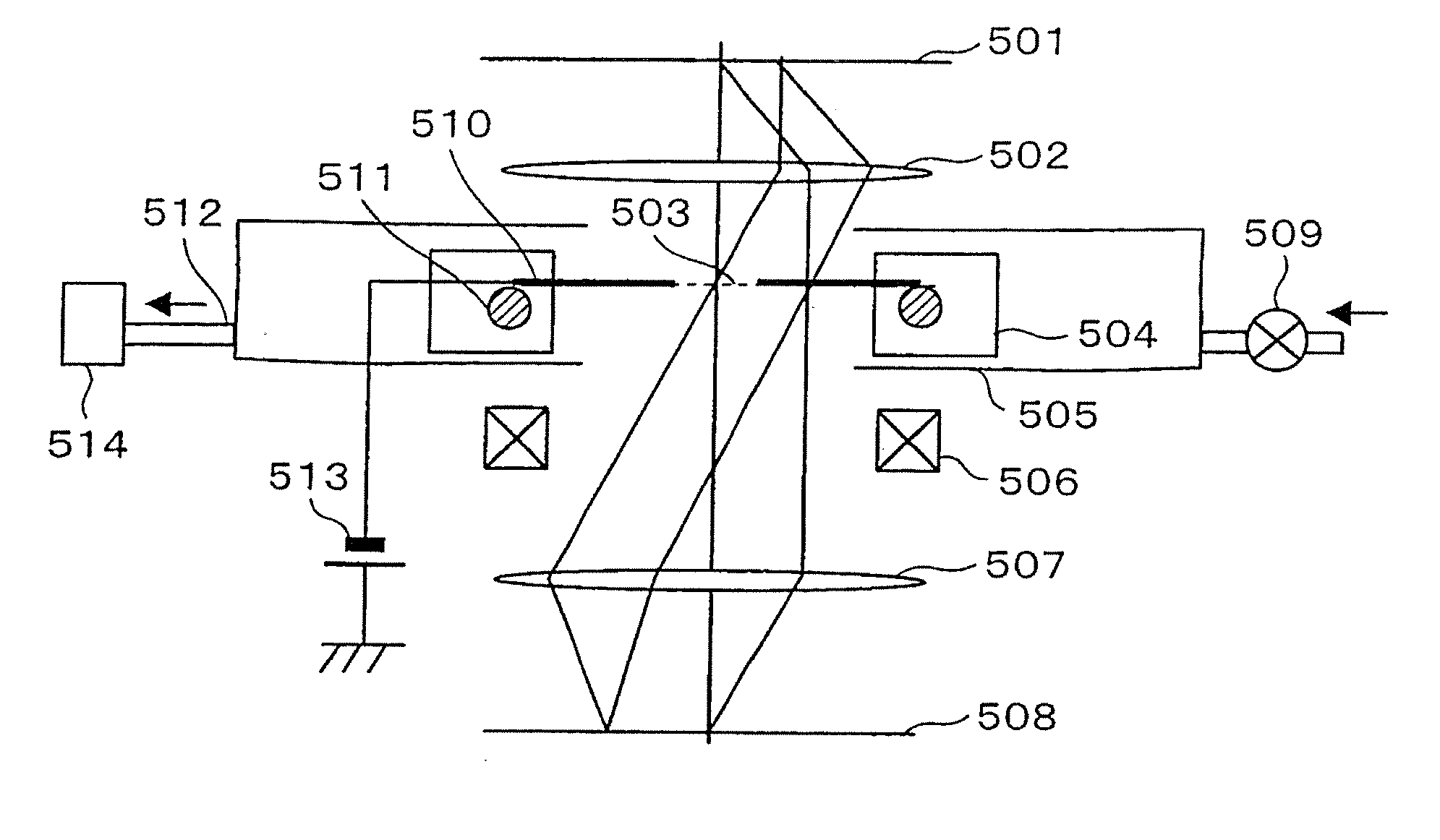
FIG. 5(a) illustrates a schematic mechanism of the present embodiment. In the present embodiment, description is given of an electron microscope including a phase plate in the vicinity of a diffraction plane of an electron beam. There is provided a function of causing the phase plate holder 504 to heat, tilt, and displace the phase plate 510 and to apply a voltage to the phase plate 510. The phase plate 510 has a mechanism which is inserted from the outside into the phase plate chamber 505 by using the phase plate holder 504. The phase plate chamber 505 has a hole having a diameter which is large enough to allow the electron beam to pass therethrough. In addition, the phase plate chamber 505 includes: a gas introducing mechanism including a gas introduction valve adjusting function 509 and a gas introduction pipe 516; and an exhausting mechanism including an exhaust pipe 512 and an exhaust apparatus 514.

The phase plate 510 has a shape as illustrated in FIG. 5(b), and is a circular p...

embodiment 2

Embodiment 2 is illustrated in FIG. 12. In the present embodiment, there is disclosed a scanning electron microscope which converges an electron beam on a sample surface for observation, the scanning electron microscope including a phase adjusting apparatus which adjusts a phase difference on the sample surface between electrons having different irradiation angles, which is caused by a spherical aberration of a lens provided between a sample and an electron source.

According to the present embodiment, it is possible to improve the coherence when a large diaphragm is used and the irradiation angle is made larger, so that the brightness of an electron probe is improved. As a result, high-sensitivity analysis and photographing of an image with a high S / N ratio are possible.

The use as a scanning transmission electron microscope, which is configured by providing the above-mentioned scanning electron microscope with a transmitted electron detector and a scattered electron detector, is also...


PUM

PropertyMeasurementUnit
accelerating voltageaaaaaaaaaa
electron microscopeaaaaaaaaaa
phaseaaaaaaaaaa

Abstract

An electron microscope according to the present invention includes a phase plate (510) having a thickness which changes in a radial direction, and adjusts a phase difference caused by a difference in electron beam path due to an effect of a spherical aberration when an electron beam is converged by a lens or an image of the electron beam is formed. Accordingly, the phase difference caused by the difference in electron beam path is adjusted, to thereby improve the coherence, so that a phase contrast image of transmitted electrons can be obtained at a higher resolution.

Description

TECHNICAL FIELDThe present invention relates to an electron microscope. For example, the present invention relates to a phase adjuster for providing an arbitrary phase adjusting mechanism in terms of electron beam optics. In addition, for example, the present invention relates to a spherical aberration of the electron microscope. In addition, for example, the present invention relates to a transmission electron microscope for forming an enlarged image of a sample to be observed as faithfully to its original structure as possible.BACKGROUND ARTA transmission electron microscope is an apparatus which enables the observation of an atomic-scale structure, and fulfills its function in various fields. However, an image which can be observed using the transmission electron microscope is an image formed by the interference between electron beams, and hence the observed image cannot be interpreted as it is. Therefore, simulation and the like are performed, and observation results and calcula...

Claims


Application Information

Patent Timeline
Patent Type & Authority Applications(United States)
IPC IPC(8): G01N23/04
CPCH01J37/26H01J2237/2802H01J2237/2614H01J2237/1534
Inventor NAGAOKI, ISAOTANIGAKI, TOSHIAKI
Owner HITACHI HIGH-TECH CORP
Why Eureka
Try Eureka