

Light emitting diode and manufacturing method thereof
- Summary
- Abstract
- Description
- Claims
- Application Information
AI Technical Summary
Benefits of technology
Problems solved by technology
Method used
Image

Examples
Embodiment Construction
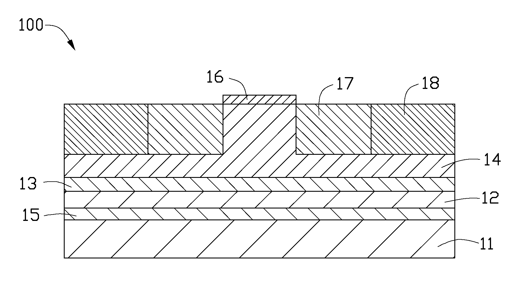
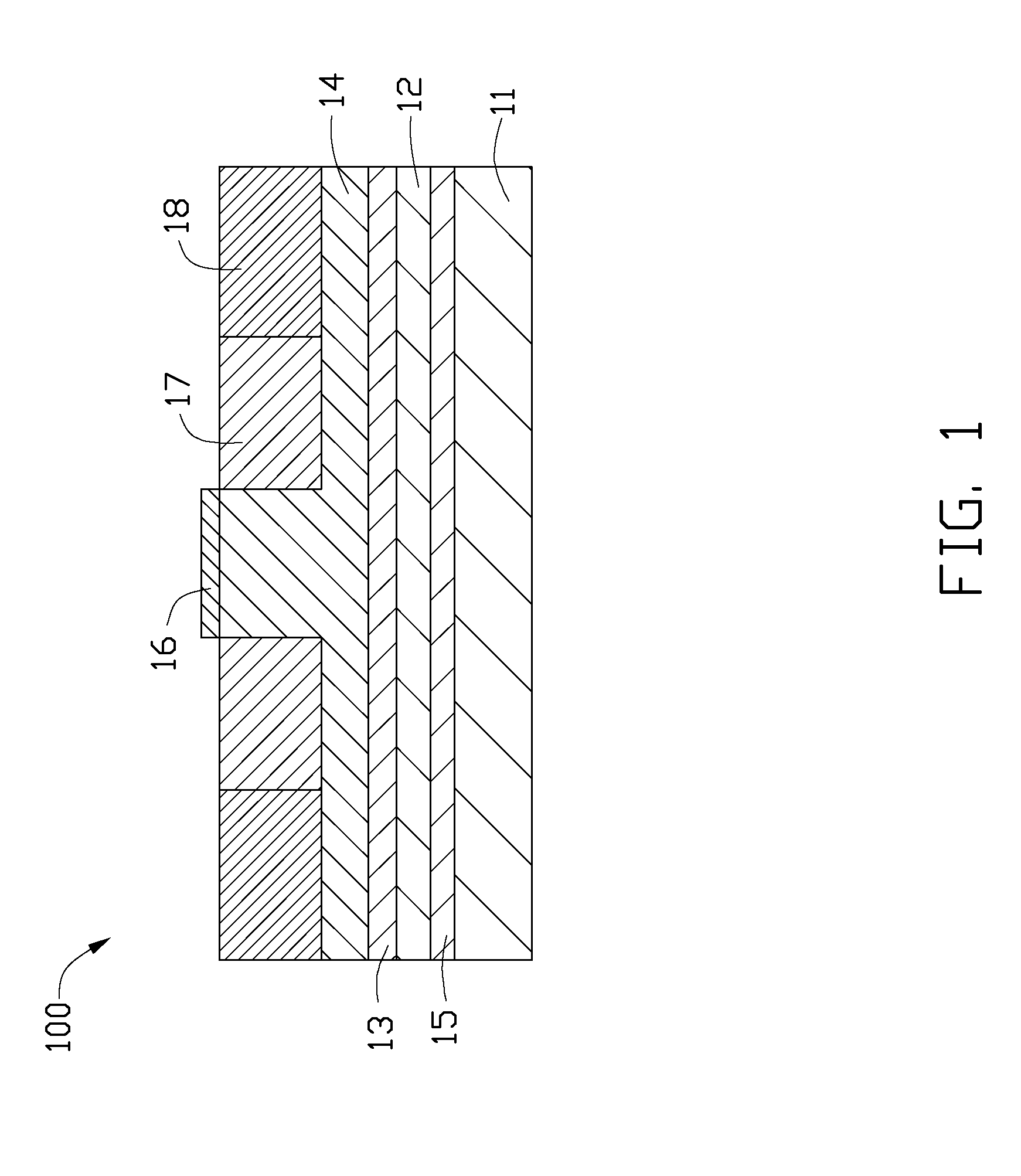
[0012]Embodiments of the LED and the method for manufacturing the LED will now be described in detail below and with reference to the drawings.
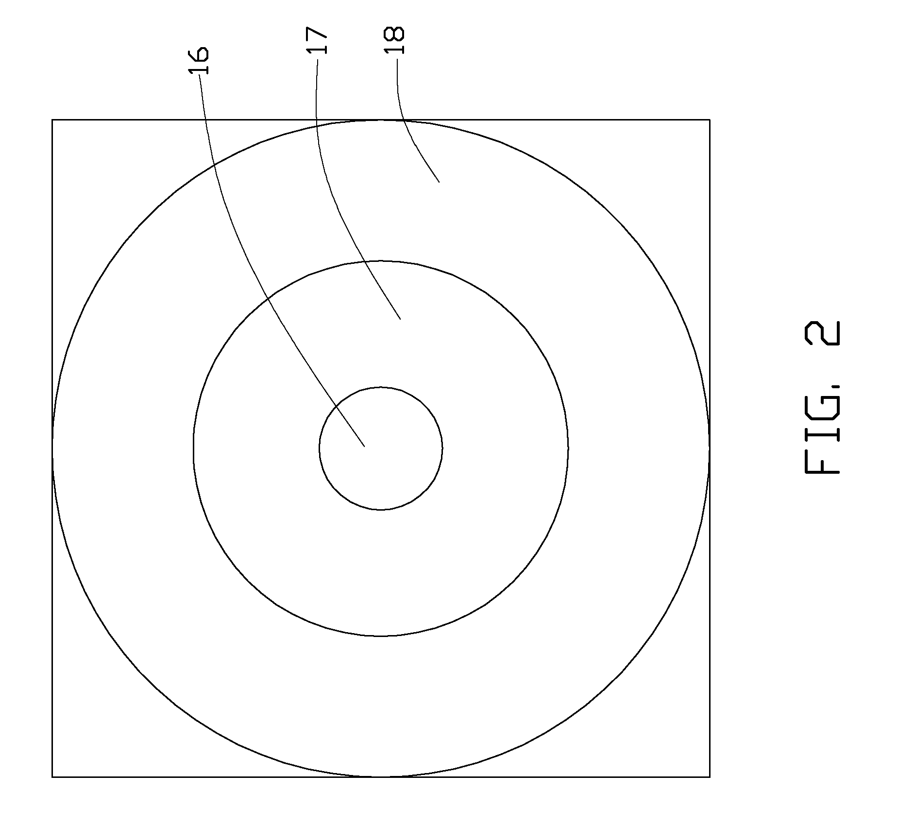
[0013]Referring to FIG. 1, an LED 100 in accordance with a first embodiment is shown. The LED 100 includes a substrate 11, a p-type GaN layer 12, an active layer 13, an n-type GaN layer 14, a reflective layer 15 and an electrode pad 16.
[0014]The substrate 11 can be made of metal with high thermal conductivity, such as copper, aluminum, nickel, silver, gold, an alloy thereof, or any other suitable metal or alloy. In this embodiment, the substrate 11 is made of nickel. In addition, the substrate 11 can be a ceramic substrate such as a silicon substrate or germanium substrate.
[0015]The p-type GaN layer 12, the active layer 13 and the n-type GaN layer 14 are sequentially stacked above the substrate 11. When a voltage is applied between the p-type GaN layer 12 and the n-type GaN layer 14, electrons in the n-type GaN layer 14 and holes in the p-typ...
PUM
 Abstract
Description
Claims
Application Information