
Successive aproximation A/D Converter

a converter and approximation technology, applied in the field of a/d converters, can solve the problems of general difficulty, inability to determine the magnitude relationship between the comparison target voltage and the input analog voltage v/sub>in /sub>, and the conversion accuracy decreases. the effect of simplifying the configuration

Inactive Publication Date: 2011-06-09
YAMAHA CORP
View PDF6 Cites 15 Cited by
  • Summary
  • Abstract
  • Description
  • Claims
  • Application Information

AI Technical Summary

Benefits of technology

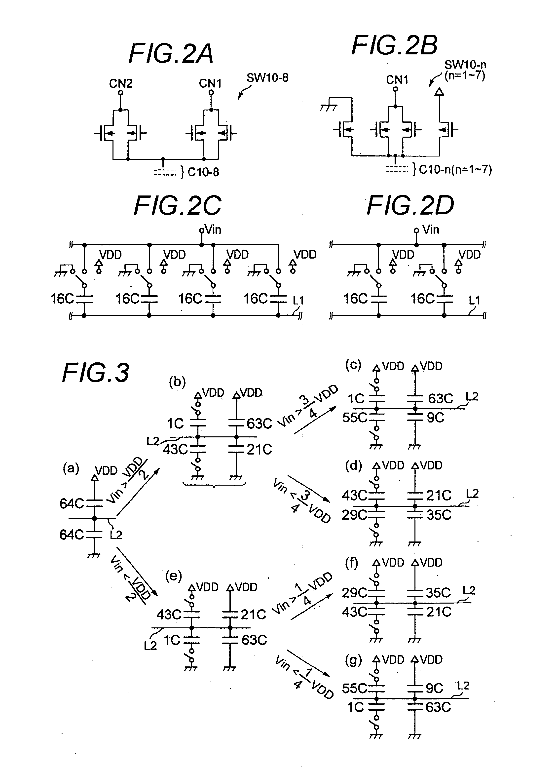
[0017]According to the former aspect, although it is necessary to perform a complicated control (and to have a configuration for realizing such a control) of adjusting the capacitances of the first and second capacitive elements in synchronism with a successive comparison operation, it is advantageous in that the influence of fluctuation of the output voltage of the high potential power supply can always be eliminated regardless of the signal value of the input analog signal. On the other hand, according to the latter aspect, although the influence of fluctuation of the output voltage of the high potential power supply can be eliminated only when the signal value of the input analog signal has a value corresponding to a specific code or a near value thereof, it is advantageous in that the configuration can be simplified compared to the former aspect.

Problems solved by technology

It is generally difficult with the resistance division-type A / D converter to realize a resolution of 8 bits or higher.
However, since the output voltage of this kind of power supply contains a ripple component, when the output voltage is low, there is a problem in that the A / D conversion accuracy decreases greatly due to the fluctuation thereof.
Therefore, if the power supply voltage fluctuates when determining the bit value of the bits other than the MSB, the magnitude relationship between the comparison target voltage and the input analog voltage Vin is not determined correctly.

Method used


Image

  • Successive aproximation A/D Converter
  • Successive aproximation A/D Converter
  • Successive aproximation A/D Converter

Examples


first embodiment

A: First Embodiment

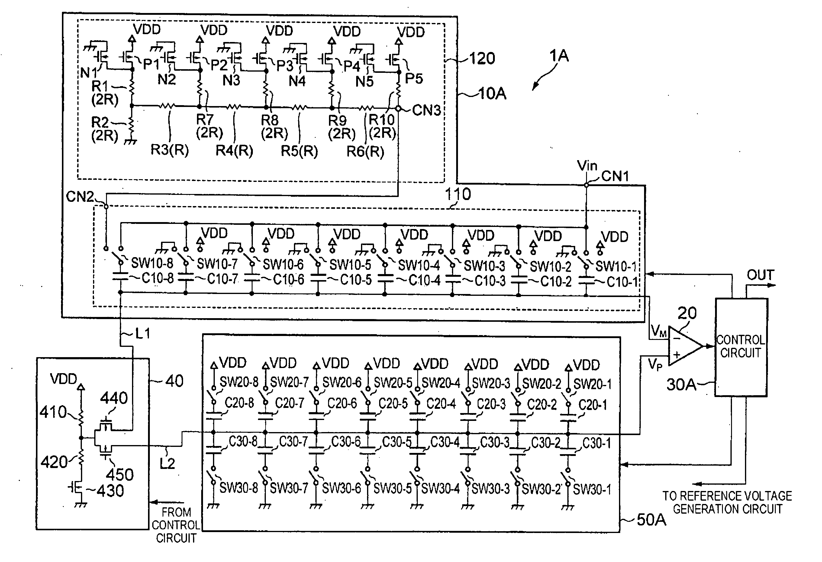
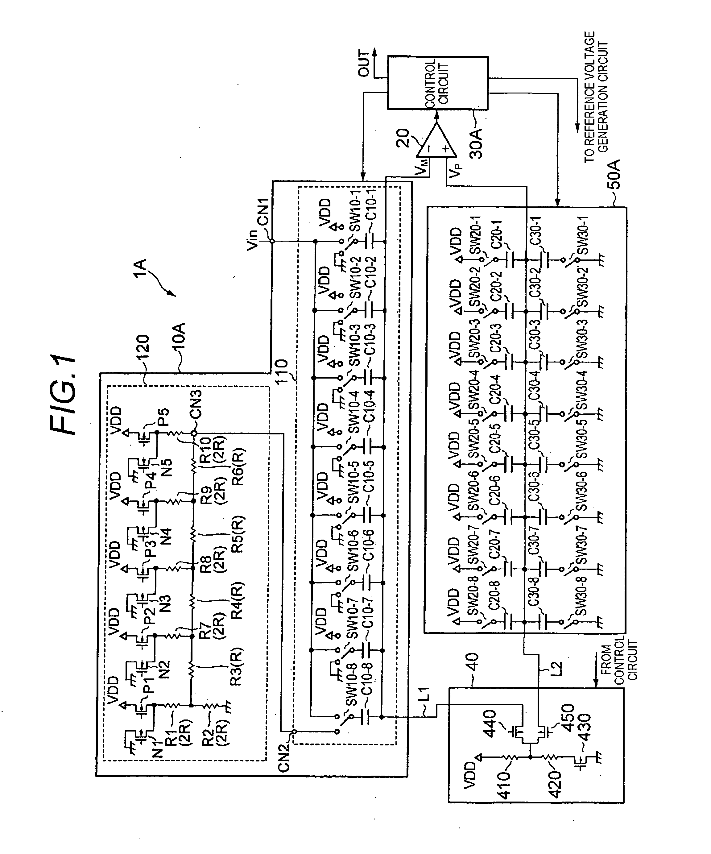
[0027]FIG. 1 is a block diagram showing a configuration example of an A / D converter 1A according to a first embodiment of the present invention.

[0028]The A / D converter 1A is a successive approximation A / D converter that converts an input analog voltage Vin to 12-bit digital data OUT and outputs the data OUT. As shown in FIG. 1, the A / D converter 1A includes a local D / A converter circuit 10A, a comparator 20, a control circuit 30A, a reference voltage generation circuit 40, and a reference voltage adjustment circuit 50A.

[0029]The function and configuration of the reference voltage generation circuit 40 are basically the same as those of a conventional successive approximation A / D converter (see FIG. 5). As shown in FIG. 1, the reference voltage generation circuit 40 is a voltage divider circuit in which resistors 410 and 420 and an N-channel field-effect transistor 430 are disposed in series between a high potential power supply that outputs a positive voltage VDD ...


PUM


Abstract

A successive approximation A / D converter, includes a reference voltage generation circuit, a sample / hold circuit, a D / A converter circuit, a comparator, and a control circuit. A potential difference between the comparison target voltage generated by the D / A converter circuit and the internal analog voltage is applied to one input terminal of the comparator through a first signal line, and the reference voltage generation circuit is connected to the other input terminal of the comparator through a second signal line and a switch. Capacitive elements are disposed between the high potential power supply and the second signal line, and between the second signal line and the low potential power supply, respectively. The control circuit turns ON the switch to charge the first and second capacitive elements during a period when the sample / hold circuit samples and holds the internal analog voltage and turns OFF the switch in response to end of the period.

Description

BACKGROUND OF THE INVENTION[0001]1. Technical Field[0002]The present invention relates to an A / D converter that converts an analog signal to digital data, and more particularly, to a successive approximation A / D converter.[0003]2. Background Art[0004]Successive approximation A / D converters sequentially compare the magnitudes of an input analog voltage with voltages (hereinafter, comparison target voltages) corresponding to ½, ¼ (or ¾) of a power supply voltage VDD to specify a comparison target voltage that is closest to the input analog voltage and output digital data representing the comparison target voltage. Successive approximation A / D converters are classified into a resistance division-type A / D converter, a charge redistribution-type A / D converter, and an A / D converter using the two types depending on a configuration of a circuit that generates comparison target voltages. It is generally difficult with the resistance division-type A / D converter to realize a resolution of 8 bi...

Claims


Application Information

Patent Timeline
IPC IPC(8): H03M1/02
CPCH03M1/0845H03M1/468H03M1/806H03M1/785H03M1/68
Inventor KAWAI, HIROTAKA
Owner YAMAHA CORP
Learn More