Wavelength-tunable optical transmitter
- Summary
- Abstract
- Description
- Claims
- Application Information
AI Technical Summary
Benefits of technology
Problems solved by technology
Method used
Image

Examples
first embodiment
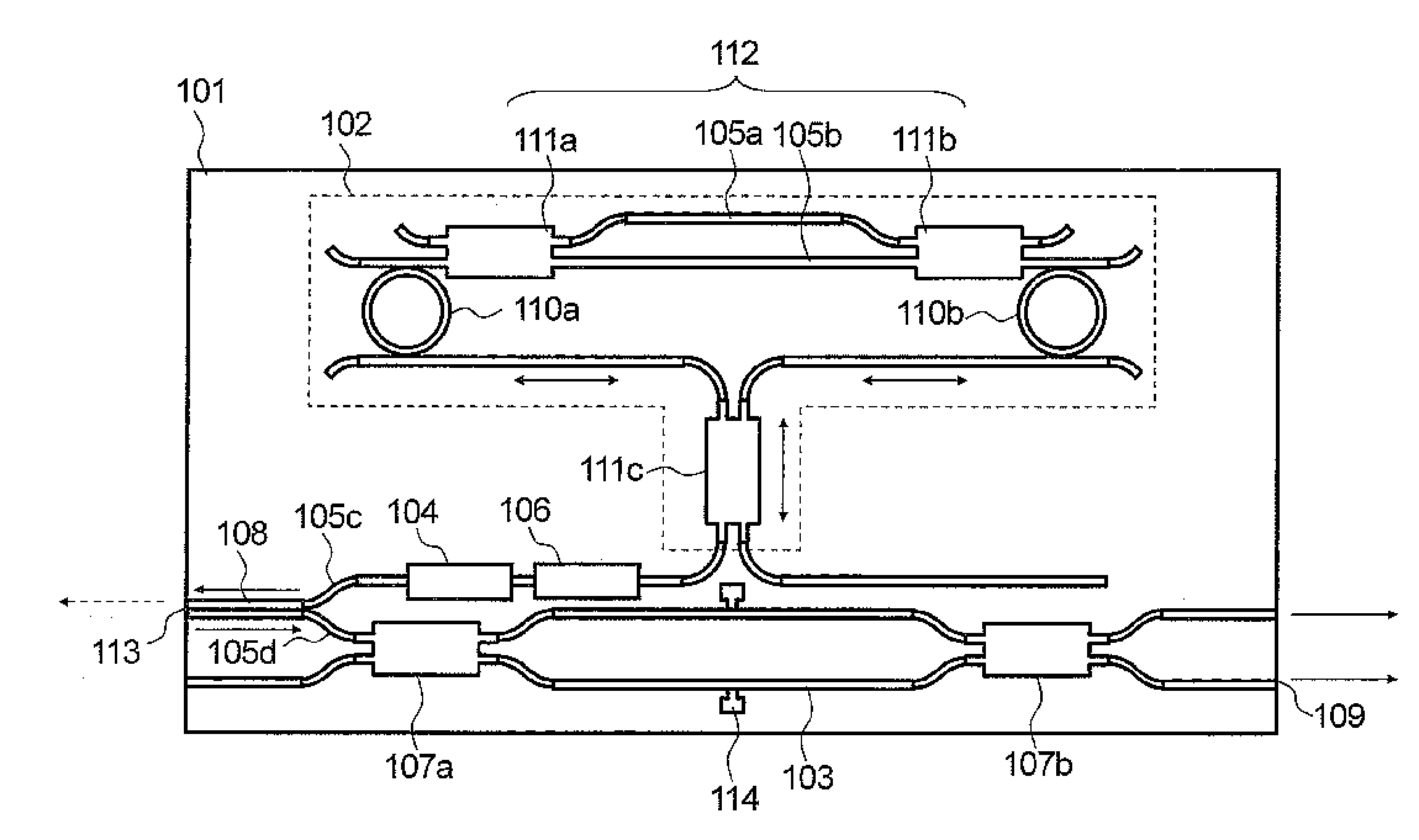
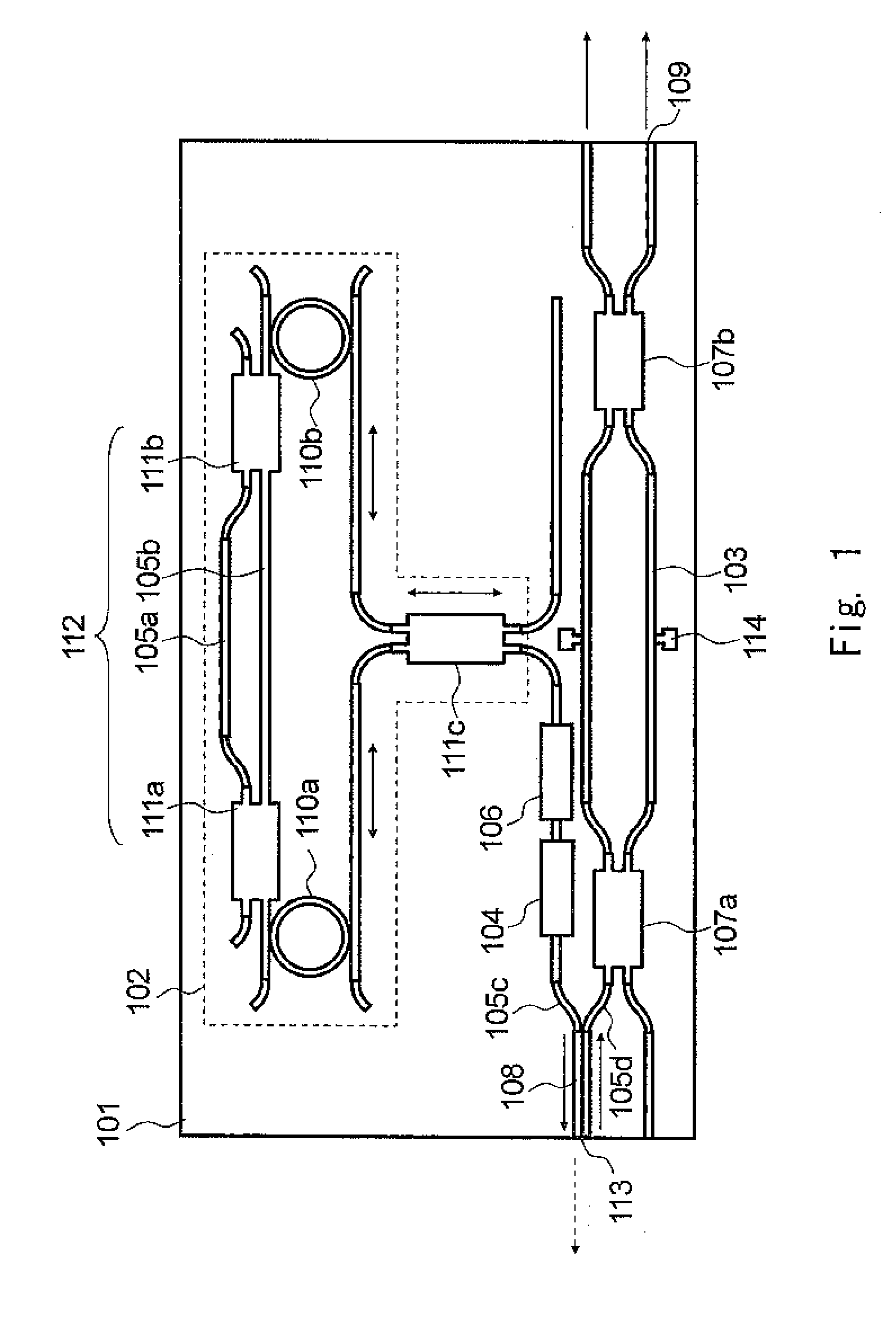
[0048]Next, a first embodiment of the present invention is described in detail with reference to the drawings. FIG. 1 is a plan view showing a structure of a wavelength-tunable optical transmitter according to the first embodiment of the present invention. The structure is described in turn below.
[0049]In the wavelength-tunable optical transmitter, a wavelength-tunable light source and an MZ optical modulator are monolithically integrated on a single semiconductor substrate 101. The wavelength-tunable light source includes a gain region 104, a phase control region 106, and a wavelength-tunable reflector 102. The components are connected by waveguides 105.
[0050]Here, the wavelength-tunable reflector 102 includes a pair of semiconductor optical resonators 110a, 110b having free spectral ranges slightly different from each other, an optical bandpass filter 112 to which an asymmetric MZ interferometer is applied, and a multiplexer / demultiplexer 111c. In the optical bandpass filter 112, ...
first example
[0055]Next, a mode for the invention 1 of the wavelength-tunable optical transmitter according to the first embodiment of the present invention is described with reference to FIG. 1. In the wavelength-tunable optical transmitter according to the mode for the invention 1, a wavelength-tunable light source and an MZ type optical modulator are monolithically integrated on a semi-insulating type semiconductor substrate 101 composed of InP.
[0056]A gain region 104 of the wavelength-tunable light source is composed of a semiconductor optical amplifier having a length of 450 μm and having a structure sandwiching an undoped InGaAsP / InGaAsP multiple quantum well active layer (10 well layers, a gain peak wavelength of 1550 nm) between a p-InP upper cladding layer and an n-InP lower cladding layer.
[0057]A wavelength-tunable reflector 102 is an optical resonator based on a semiconductor optical waveguide structure sandwiching a gain region composed of an undoped AlGaInAs / AlGaInAs multiple quantu...
second embodiment
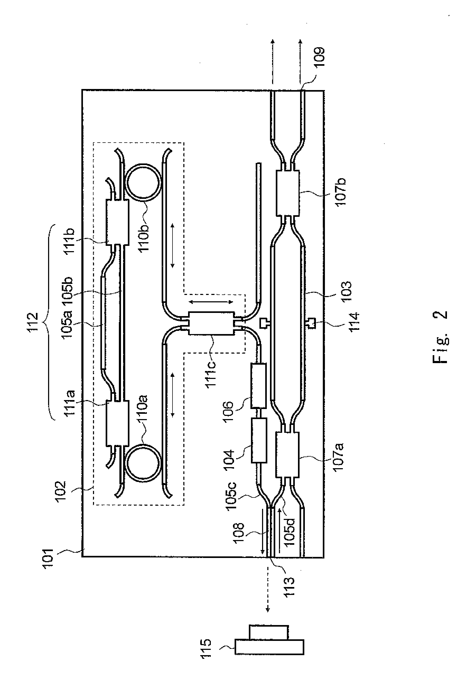
[0062]Next, a second embodiment of the present invention is described with reference to the drawings. FIG. 2 is a plan view showing a structure of a wavelength-tunable optical transmitter according to the second embodiment of the present invention. The difference from the first embodiment is that a photodetector 115 that monitors the strength of signal light leaking from the end face of the coupling region 108 is provided in the vicinity of the end face. The other configuration is the same as that of the first embodiment, and thus the explanation is omitted. According to the configuration of this embodiment, an optical output of the wavelength-tunable light source can be controlled by monitoring a photocurrent of the photodetector 115.
[0063]As described above, the wavelength-tunable optical transmitter according to the present invention can effectively solve problems such as downsizing and fabrication yield in realizing the ultra high speed optical modulator and the integrated optic...
PUM
 Abstract
Description
Claims
Application Information