Nanoporous inorganic membranes and films, methods of making and usage thereof
a technology of inorganic membranes and films, applied in the field of track etching methodologies, can solve the problems of polymer membranes that prohibit this highly demanded application
- Summary
- Abstract
- Description
- Claims
- Application Information
AI Technical Summary
Benefits of technology
Problems solved by technology
Method used
Image
Examples
Embodiment Construction
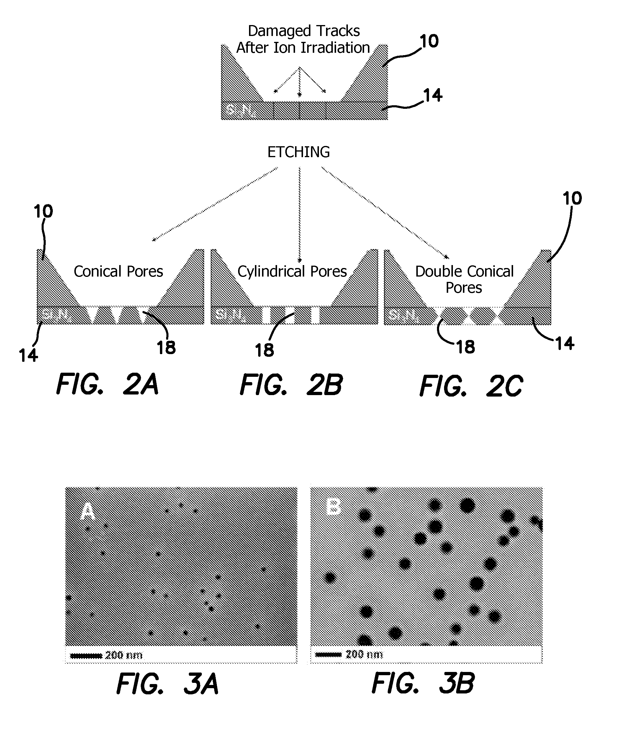
[0048]The illustrated embodiment discloses a fabrication method using silicon nitride films as an example. The same approach can be used for preparation of straight, well-defined pores in other inorganic films, e.g. silica, alumina and similar materials. The production process starts with the product which is well described in the literature and can be bought or easily made. We used homemade starting materials. All the dimensions in the following figures are not to scale and just serve as an example.
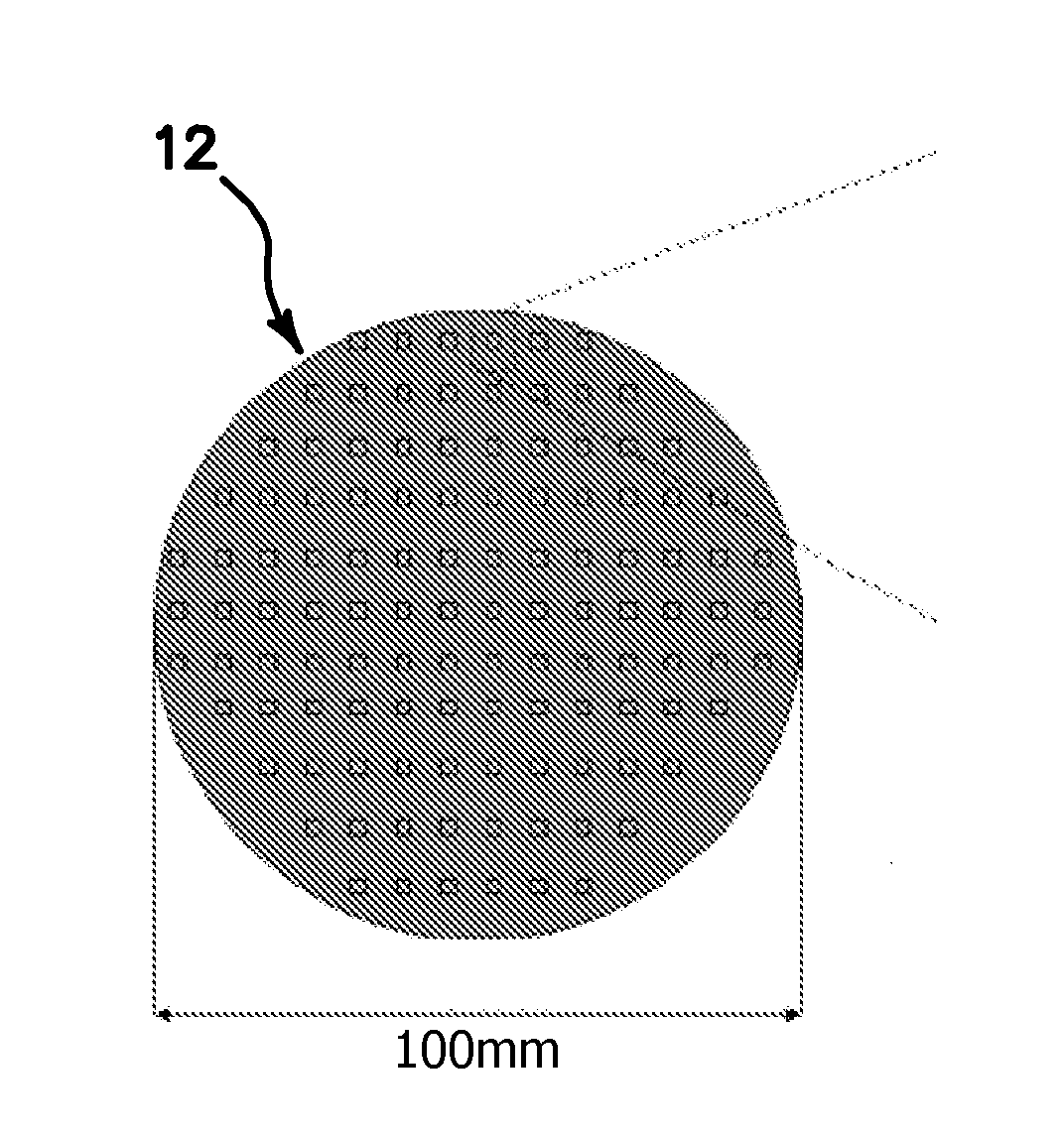
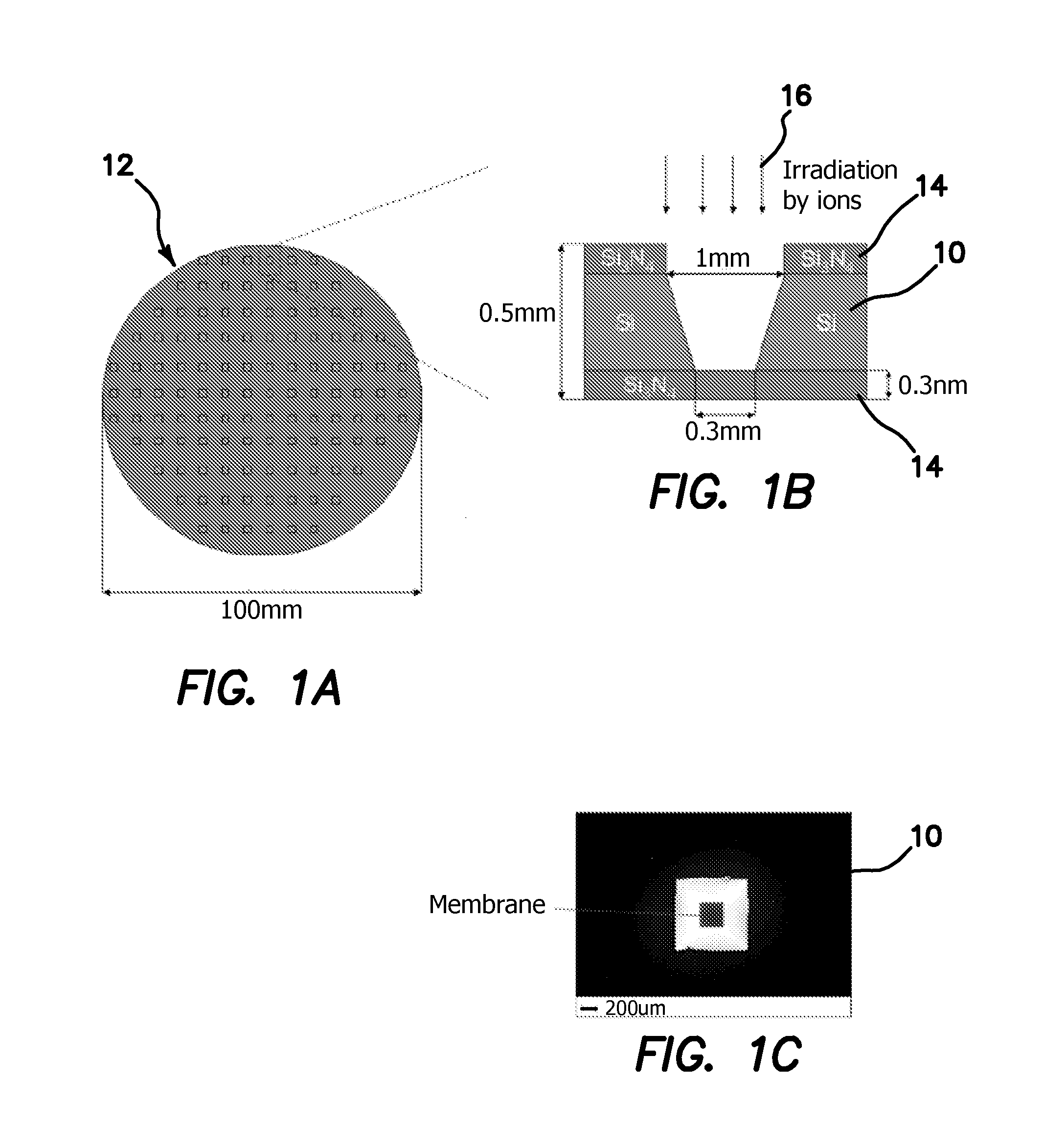
[0049]As shown in FIGS. 1A-1C using standard lithography techniques, supported patterned membranes 10 are made on a silicon wafer 12 covered or supported on its upper and lower surfaces with desired dielectric layer 14 (SixNy for example). The supported patterned membranes 10 are then irradiated with energetic ions 16 diagrammatically illustrated in FIG. 1B. The irradiation can be done from different sides of the membrane 10. FIG. 1B shows an example in which the irradiation is performed...
PUM
 Abstract
Description
Claims
Application Information


