

Semiconductor device and method for manufacturing the same
- Summary
- Abstract
- Description
- Claims
- Application Information
AI Technical Summary
Benefits of technology
Problems solved by technology
Method used
Image

Examples
embodiment 1
[0049]An example of a method for manufacturing a semiconductor device will be described.
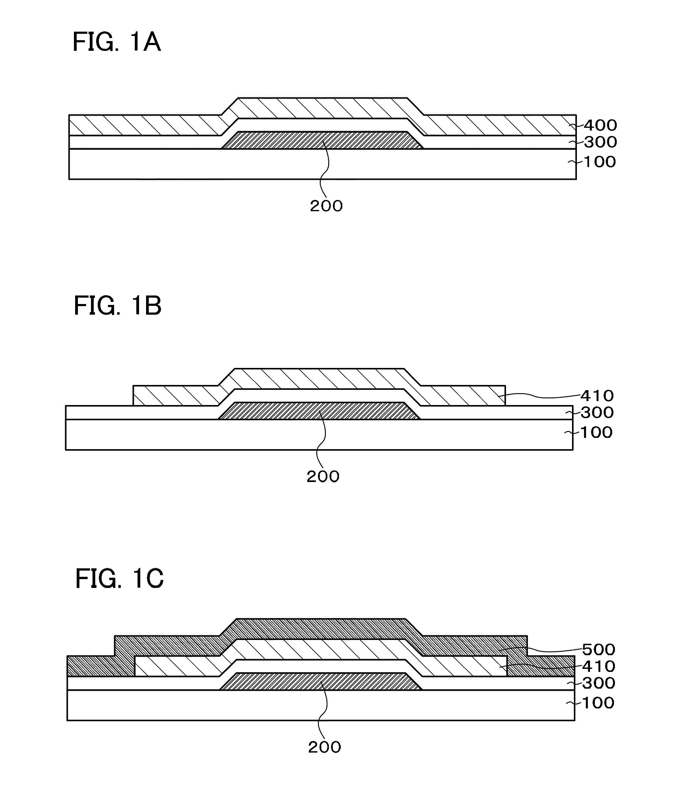
[0050]First, a gate electrode 200 is formed over a substrate 100 having an insulating surface. Then, a gate insulating layer 300 is formed over the gate electrode 200, and an oxide semiconductor layer 400 is formed over the gate insulating layer 300 (FIG. 1A).
[0051]As the substrate, any material can be used. For example, a glass substrate, a quartz substrate, a metal substrate, a plastic substrate, or a semiconductor substrate can be used, but the substrate is not limited to these examples.
[0052]In the case where an insulating substrate is used as the substrate, the substrate has an insulating surface.
[0053]On the other hand, in the case where a metal substrate, a semiconductor substrate, or the like is used as the substrate, the substrate can have an insulating surface when a base insulating layer is formed over the substrate.
[0054]Note that a base insulating layer may be formed over the substra...
embodiment 2
[0171]In this embodiment, a semiconductor device including a transistor which has a structure different from that of the transistor in Embodiment 1 will be described.
[0172]Note that materials or the like of the layers are the same as those in Embodiment 1.
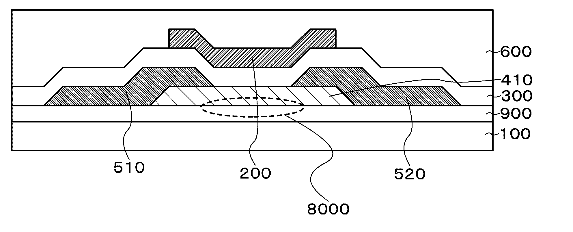
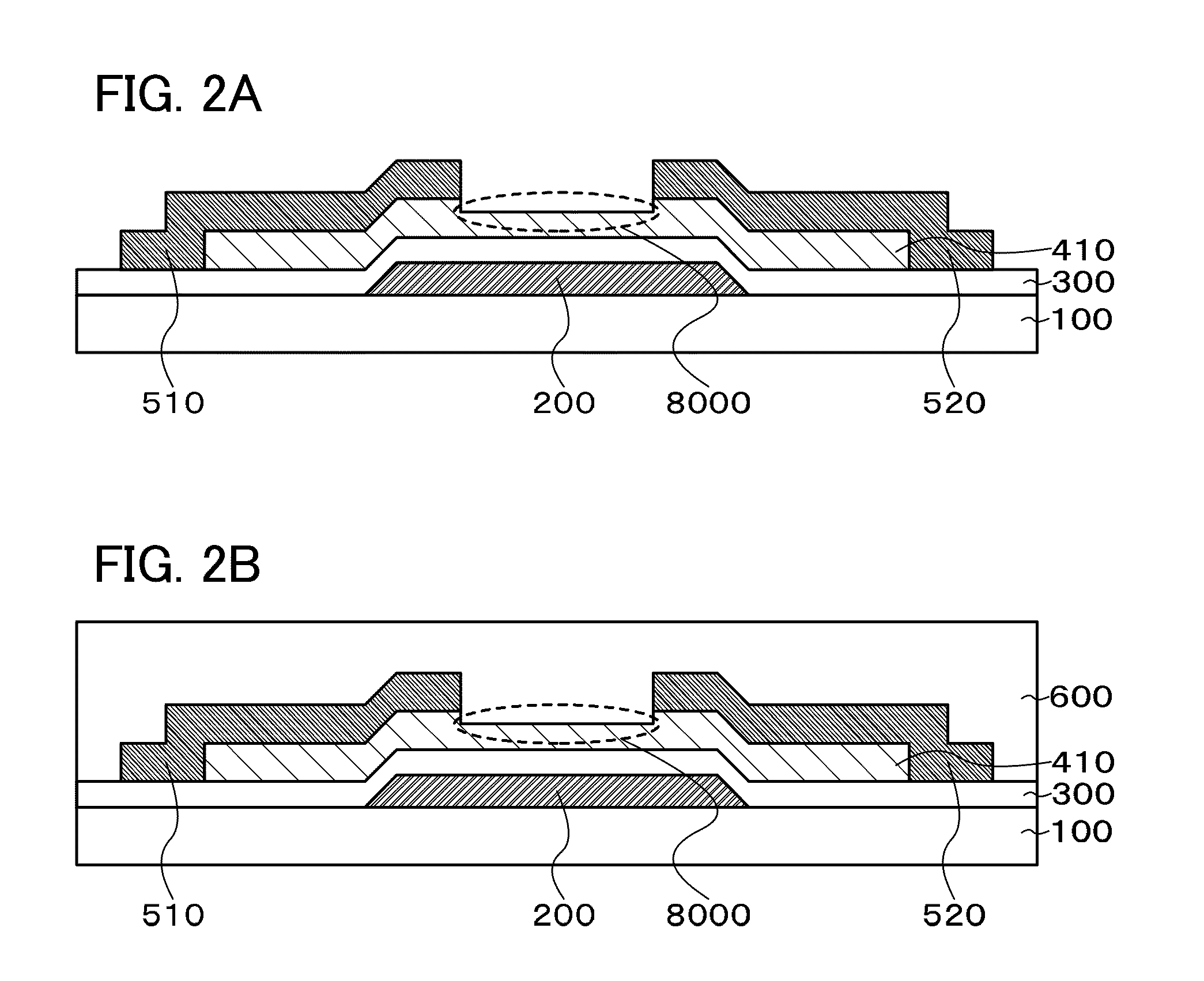
[0173]A transistor in FIG. 4A is a bottom-gate bottom-contact (BGBC) transistor, and includes the gate electrode 200 provided over the substrate 100 having an insulating surface; the gate insulating layer 300 provided over the gate electrode 200; the contact electrode 510 and the contact electrode 520 provided over the gate insulating layer 300; and the oxide semiconductor layer 410 (island shape) provided over the gate insulating layer 300, the contact electrode 510, and the contact electrode 520.
[0174]Note that the insulating layer 600 is provided to cover the transistor.
[0175]A portion surrounded by the dashed line 8000 serves as a back channel.
[0176]A transistor in FIG. 4B is a top-gate transistor, and includes the oxide semico...
embodiment 3
[0207]An example of a method for manufacturing the semiconductor device in FIG. 4A will be described.
[0208]Note that materials, conditions of heat treatment, and the like are the same as those in another embodiment.
[0209]The gate electrode 200 is formed over the substrate 100 having an insulating surface. Then, the gate insulating layer 300 is formed over the gate electrode 200, and the contact electrode 510 and the contact electrode 520 are formed over the gate insulating layer 300 (FIG. 5A).
[0210]Next, the oxide semiconductor layer 400 is formed over the gate insulating layer 300, the contact electrode 510, and the contact electrode 520 (FIG. 5B).
[0211]Next, the oxide semiconductor layer is subjected to first heat treatment.
[0212]The conditions of the first heat treatment are the same as those in Embodiment 1.
[0213]The first heat treatment may be performed after the oxide semiconductor layer 400 is etched into an island shape to form the oxide semiconductor layer 410.
[0214]However...
PUM
 Abstract
Description
Claims
Application Information