
Semiconductor device and method of manufacturing semiconductor device

a semiconductor device and semiconductor technology, applied in semiconductor devices, semiconductor/solid-state device details, electrical apparatus, etc., can solve the problems of difficult cutting and difficult narrowing of cutting locations, and achieve the effect of easy cutting of electrical fuse and increasing heat generation of cutting portion

Active Publication Date: 2011-06-16
RENESAS ELECTRONICS CORP
View PDF2 Cites 12 Cited by
  • Summary
  • Abstract
  • Description
  • Claims
  • Application Information

AI Technical Summary

Benefits of technology

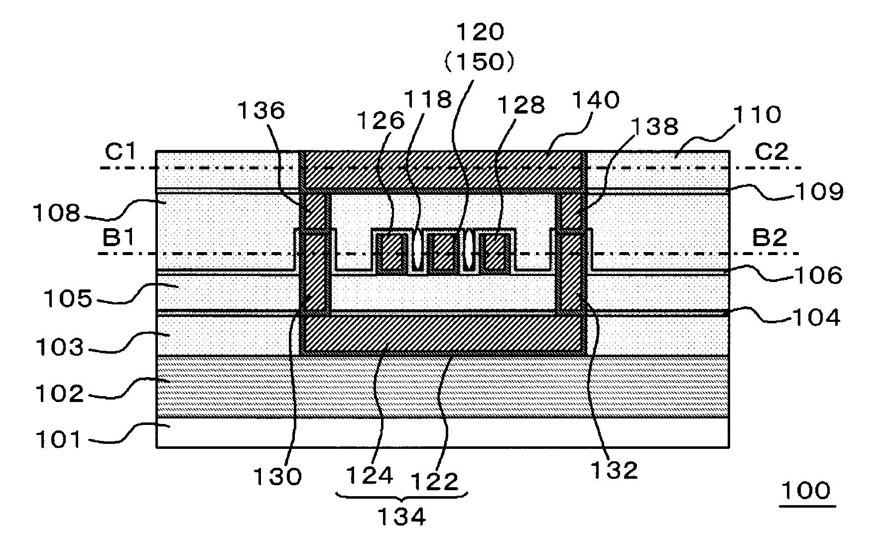
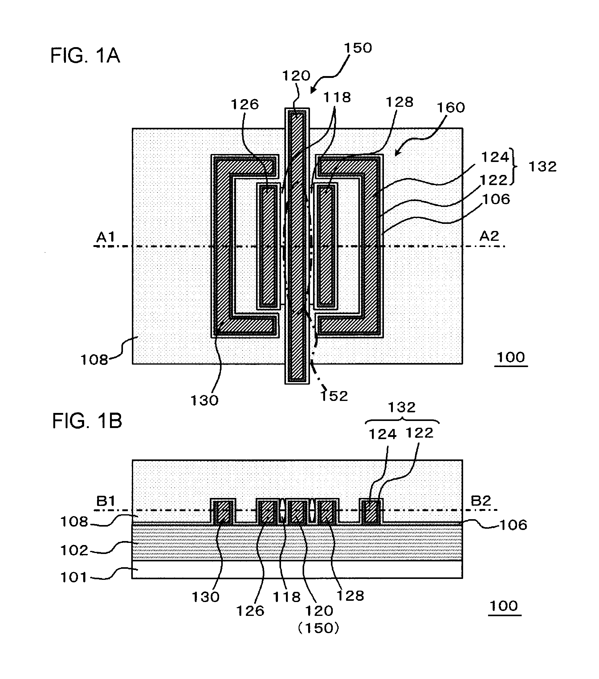
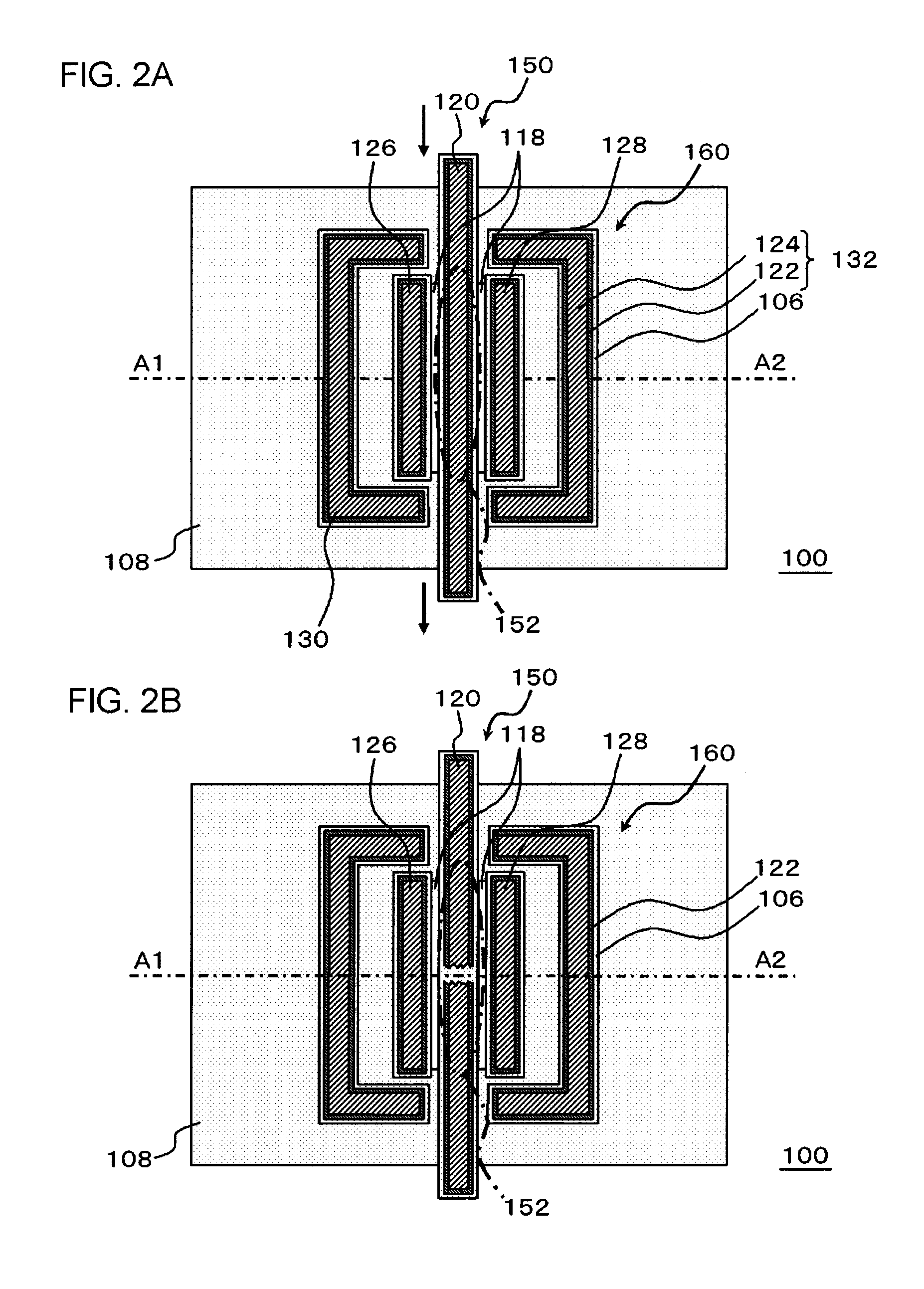
[0014]According to such a configuration, an insulating interlayer does not exist in both sides of the cutting portion of the electrical fuse, and the air gaps having a lower thermal conductivity than the insulating interlayer are provided therein. For this reason, when the electrical fuse is cut by causing a current to flow into the electrical fuse, the air gaps function as a heat blocking region. Thereby, it is possible to reduce heat dissipation from the cutting portion, to cause the cutting portion to effectively generate heat, and to easily perform the meltdown of the electrical fuse.
[0016]According to the invention, it is possible to easily cut the electrical fuse by increasing the heat generation of the cutting portion when a current is caused to flow into the electrical fuse.

Problems solved by technology

However, in the method of cutting the fuse with a laser, it is difficult to narrow down the cutting location.
Especially, when the electrical fuse is formed of, for example, a material having a strong electromigration resistance such as copper, there is a problem that cutting is difficult to occur.

Method used


Image

  • Semiconductor device and method of manufacturing semiconductor device
  • Semiconductor device and method of manufacturing semiconductor device
  • Semiconductor device and method of manufacturing semiconductor device

Examples


Embodiment Construction

[0029]The invention will be now described herein with reference to illustrative embodiments. Those skilled in the art will recognize that many alternative embodiments can be accomplished using the teachings of the present invention and that the invention is not limited to the embodiments illustrated for explanatory purposes.

[0030]Hereinafter, the embodiment of the invention will be described with reference to the accompanying drawings. In all the drawings, like elements are referenced by like reference numerals and descriptions thereof will not be repeated.

[0031]FIGS. 1A and 1B are diagrams illustrating an example of a configuration of a semiconductor device according to the embodiment. FIG. 1A is a plan cross-sectional view of a semiconductor device 100, and FIG. 1B is a cross-sectional view of the semiconductor device 100. FIG. 1A corresponds to a cross-sectional view taken along the line B1-B2 shown in FIG. 1B, and FIG. 1B corresponds to a cross-sectional view taken along the lin...


PUM


Abstract

A semiconductor device include an insulating interlayer formed over a substrate; an electrical fuse which is composed of a first wiring formed in the insulating interlayer, and has a cutting portion; and a second wiring and a third wiring, formed respectively on both sides of the cutting portion to extend along the cutting portion in the same layer as the first wiring. Air gaps formed to extend along the cutting portion are respectively provided between the cutting portion and the second wiring and between the cutting portion and the third wiring.

Description

[0001]This application is based on Japanese patent application No. 2009-280474, the content of which is incorporated hereinto by reference.BACKGROUND[0002]1. Technical Field[0003]The present invention relates to a semiconductor device and a method of manufacturing the semiconductor device, and particularly to a semiconductor device including an electrical fuse and a method of manufacturing the semiconductor device.[0004]2. Related Art[0005]Hitherto, in semiconductor devices having a multilayer wiring structure in which a wiring and an insulating interlayer are used, the interconnect is buried in the inside of a groove provided in the insulating interlayer. The interconnect having such a wiring structure can be used as a fuse.[0006]As one method of cutting the fuse, there is a method of irradiating a cutting portion of the fuse with a laser. Japanese Unexamined Patent Publication No. H11-97542 discloses a configuration in which the fuse is cut by laser irradiation. Here, as shown in ...

Claims


Application Information

Patent Timeline
Patent Type & Authority Applications(United States)
IPC IPC(8): H01L23/525H01L21/768
CPCH01L23/5256H01L2924/0002H01L2924/00
Inventor ODA, NORIAKI
Owner RENESAS ELECTRONICS CORP
Learn More