Inspection system

a technology of inspection system and inspection interval, applied in the field of inspection system, can solve the problem of relativly difficult to significantly shorten the exposure interval, and achieve the effect of reducing the cause of noise, reducing the cost, and flexible arithmetic processing

Inactive Publication Date: 2011-06-16
KDE CORP
View PDF20 Cites 17 Cited by
  • Summary
  • Abstract
  • Description
  • Claims
  • Application Information

AI Technical Summary

Benefits of technology

[0018]In accordance with this invention, since the detected light intensity value from each of the imaging elements is stored once in the image storage area every time the image is taken and a calculation is conducted on the data stored in the image storage area, merits can be enjoyed such that there is a lot of flexibility in an arithmetic processing so that various processing can be conducted easily compared with a case that data for every imaging is automatically integrated like the TDI. In addition, since an inexpensive area image sensor such as a CMOS sensor can be used as the imaging element, a cost can be reduced.
[0019]Furthermore, since each optical distortion amount calculated at the identical position of the object is measured at portions where the grid pattern is different, it is possible to reduce a cause of the noise such as the fluctuation of the width of the bright section and the dark section of the grid pattern, the fluctuation of the width (the pitch width) of the grid units, or dust on the grid pattern, and only the optical distortion of the glass board can be emphasized by integrating the amount of the optical distortion. Then an S / N ratio is improved so that a measurement can be conducted accurately.

Problems solved by technology

Since it is not possible for this kind of line sensor to conduct a next exposure until an electric charge charged to the CCD is read out and reset, it is relatively difficult to significantly shorten an interval of exposure, namely, an imaging interval, if a reset time is also included.

Method used


Image

  • Inspection system
  • Inspection system
  • Inspection system

Examples


Embodiment Construction

[0051]One embodiment of the present claimed invention will be explained with reference to drawings.

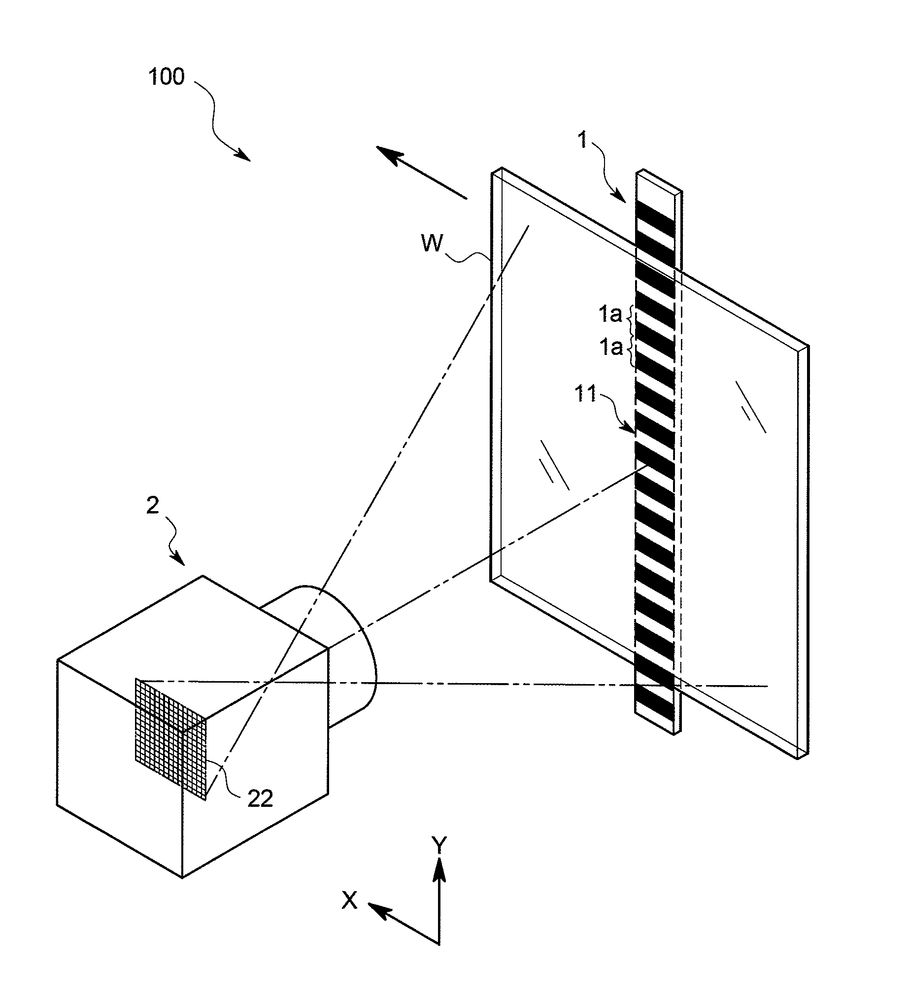
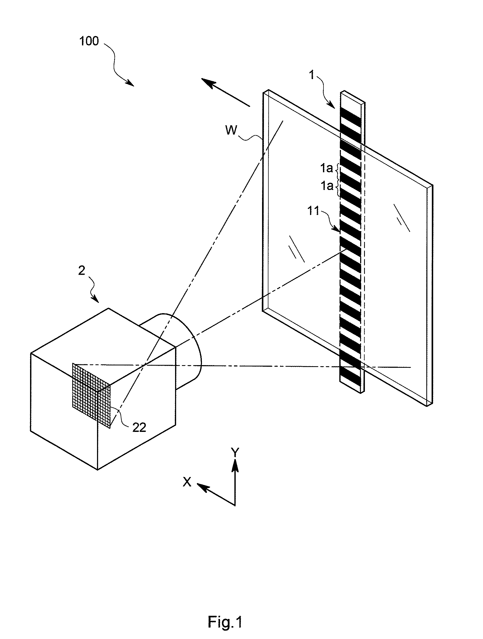
[0052]An inspection system 100 in accordance with this invention comprises, as shown in FIG. 1, a grid pattern forming device 1 and an imaging device 2 and is so arranged to move a transparent glass board W, which is an object to be inspected, in one direction between the grid pattern forming device 1 and the imaging device 2 by means of a transporting device, not shown in drawings, for scanning and imaging.

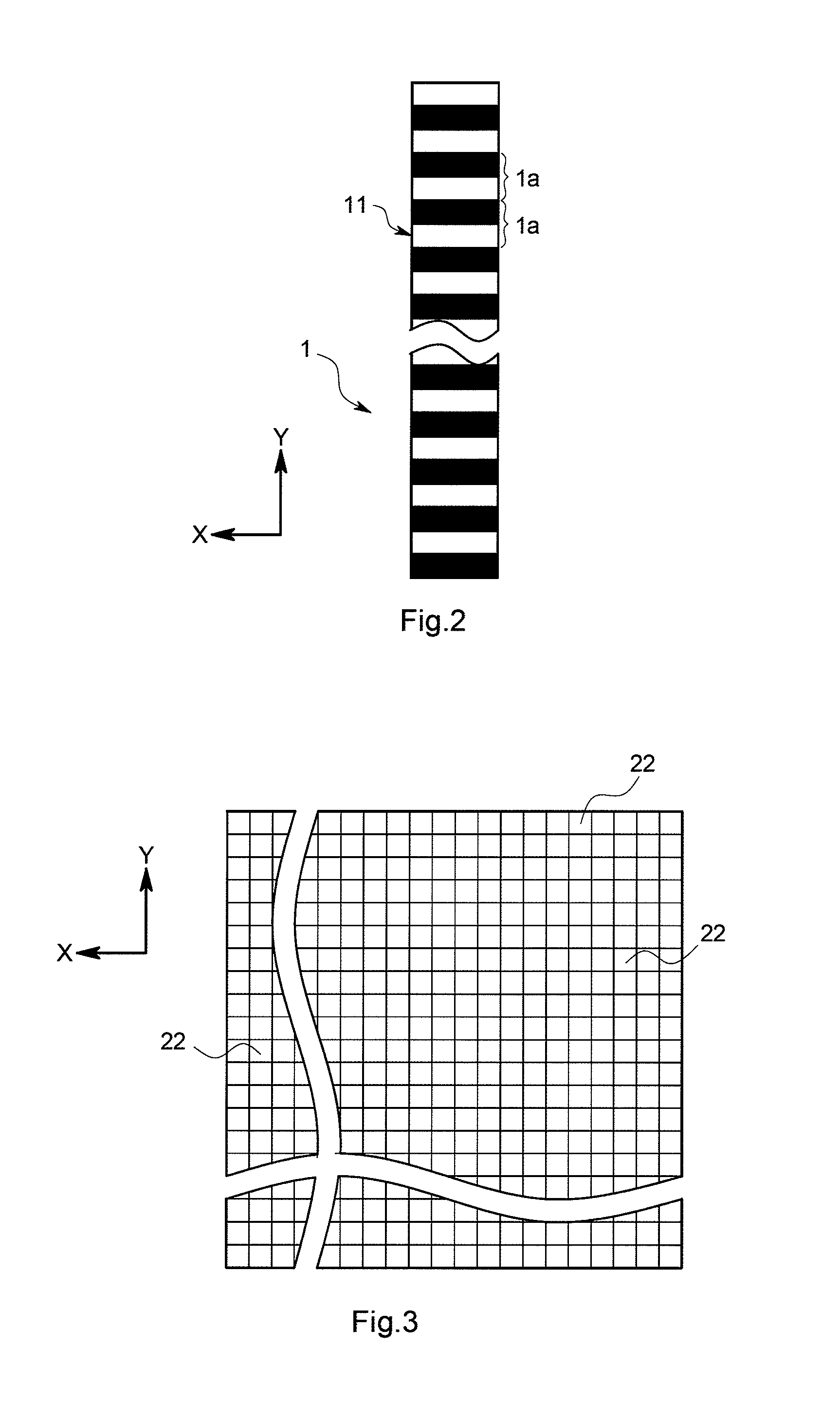
[0053]As shown in FIG. 1 and FIG. 2, the grid pattern forming device 1 forms a grid pattern 11 comprising continuous multiple grid units 1a each of which comprises a bright section and a dark section having a constant width. In this embodiment, the grid pattern 11 is depicted on a long rectangular plate. In addition, for example, the long rectangular plate may be backlit from behind or a grid pattern may be formed by arranging a light source such as an LED or a fluorescent light and...


PUM


Abstract

An inspection system is provided that can calculate highly accurate data for inspection having a high S/N ratio with high freedom. In order to attain this, an imaging timing is adjusted to synchronize a time for a projected image of an object to move by “m” pixels (“m” is an integer number greater than or equal to 1) in the X-axis direction on imaging elements, with an imaging time interval, and partial image data imaged at the identical inspection position on the object is specified from each unit of two-dimensional image data based on the object appearing deviated by “m” pixels in the X-axis direction in each unit of the two-dimensional image data imaged at each of the imaging timings, and data for inspection in which a noise reducing processing is conducted at the inspection position is produced based on each section of the partial image data.

Description

FIELD OF THE ART[0001]This invention relates to an inspection system to extract and inspect a distortion existing inside of a transparent platy body such as a glass plate or a flaw or a foreign material (hereinafter also collectively called as a defect) existing on a surface of a mirror-finished platy body based on an imaged image.BACKGROUND ART[0002]A CCD is often utilized as a line sensor for this kind of the inspection system. The line sensor has an arrangement wherein multiple photodiodes are arranged in line and CCDs are arranged in parallel to correspond to each of the photo diodes. Then, electric charge generated due to exposure of the photodiode is charged to the CCD and the charged electric charge is read out respectively so that a line of the image data is produced.[0003]Since it is not possible for this kind of line sensor to conduct a next exposure until an electric charge charged to the CCD is read out and reset, it is relatively difficult to significantly shorten an in...

Claims


Application Information

Patent Timeline
Patent Type & Authority Applications(United States)
IPC IPC(8): H04N7/18
CPCG01N21/896H04N7/18G01N21/958
Inventor MIYAKE, ATSUSHI
Owner KDE CORP
Why Eureka
Try Eureka