Flip-chip package substrate with a high-density layout

a technology of flip-chip and package substrate, which is applied in the direction of semiconductor devices, semiconductor/solid-state device details, electrical equipment, etc., can solve the problems of reducing the space utilization of the upper affecting the flexibility of the trace layout and the function, and affecting the grounding layer and power source layer on the inner surface of the substrate, so as to improve the flexibility of the trace layout and the function, and maintain the consistency of electricity

Inactive Publication Date: 2005-11-10
ADVANCED SEMICON ENG INC
View PDF8 Cites 105 Cited by
  • Summary
  • Abstract
  • Description
  • Claims
  • Application Information

AI Technical Summary

Benefits of technology

[0006] It is therefore an object of the invention to provide a flip-chip package substrate with a high density layout, which improves the flexibility of the trace layout and the function of the high-density layout and keeps the consistency of electricity and heat-effect of the flip-chip package substrate.
[0007] The invention achieves the above-identified object by providing a flip-chip package substrate with a high density layout. A flip-chip region is disposed on an upper surface of the substrate. The substrate includes a number of pads and a number of traces. The traces are disposed in the flip-chip region. At least one of the pads has a short axis and a long axis which are perpendicular to each other, so that the distance between the elongated pad and the pad adjacent thereto is not smaller than two thirds of the length of the short axis, and that at least two of the traces pass through the clearance between the elongated pad and the pad adjacent thereto. Therefore, the flexibility of the trace layout and the function of the high-density layout are improved.
[0008] The invention achieves the above-identified object by providing another flip-chip package substrate with a high-density layout. The substrate includes a number of pads and a number of traces. The pads and the traces are disposed on an upper surface of the substrate. When the pitch between two adjacent pads is not larger than 200 micrometers, the edge distance between the adjacent pads is over 80 micrometers. The adjacent pads are non-circular and elongated, and the exposed area of each pad is not smaller than 6000 squared micrometers (μm2), so that the electricity and heat-effect of the flip-chip package substrate remain consistent.
[0009] The invention achieves the above-identified object by further providing a flip-chip package substrate with a high-density layout. The substrate includes a number of pads, a number of through holes and a number of traces connecting the pads and the through holes. The upper surface of the substrate includes a flip-chip region and a peripheral region. A number of pads are aligned in matrix in the flip-chip region. Under the circumstances of having the same exposed area and the same pitch, at least a pad has a short axis and a long axis which are perpendicular to each other, so that the distance between the elongated pad and the pad adjacent thereto is not smaller than two thirds of the length of the short axis for at least two trace pass through the clearance between the elongated pad and the pad adjacent thereto, and that the through holes can be fanned out and aligned on the edge of the substrate to improve the high-density layout design of the substrate.

Problems solved by technology

Therefore, a large number of through holes need to be disposed in the flip-chip region, which is on the upper surface of the substrate, for the pads disposed in inner rows to be fanned out via an additional circuit layer disposed on the inner surface, not only incurring extra costs to the manufacturing of the substrate but also reducing the space usage of the upper surface of the substrate.
Furthermore, the grounding layer and power source layer on the inner surface of the substrate are also affected.

Method used


Image

  • Flip-chip package substrate with a high-density layout
  • Flip-chip package substrate with a high-density layout
  • Flip-chip package substrate with a high-density layout

Examples


Embodiment Construction

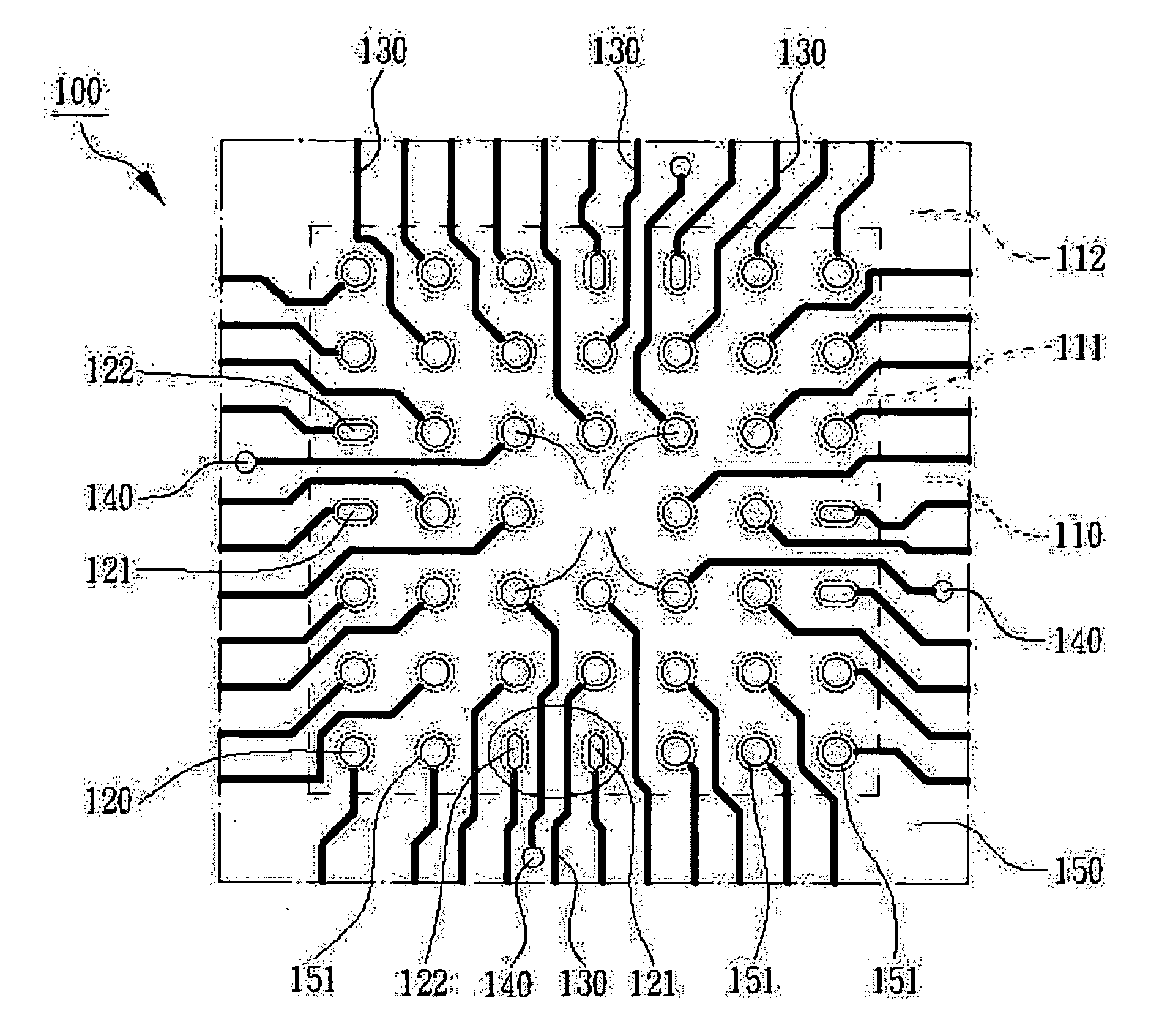
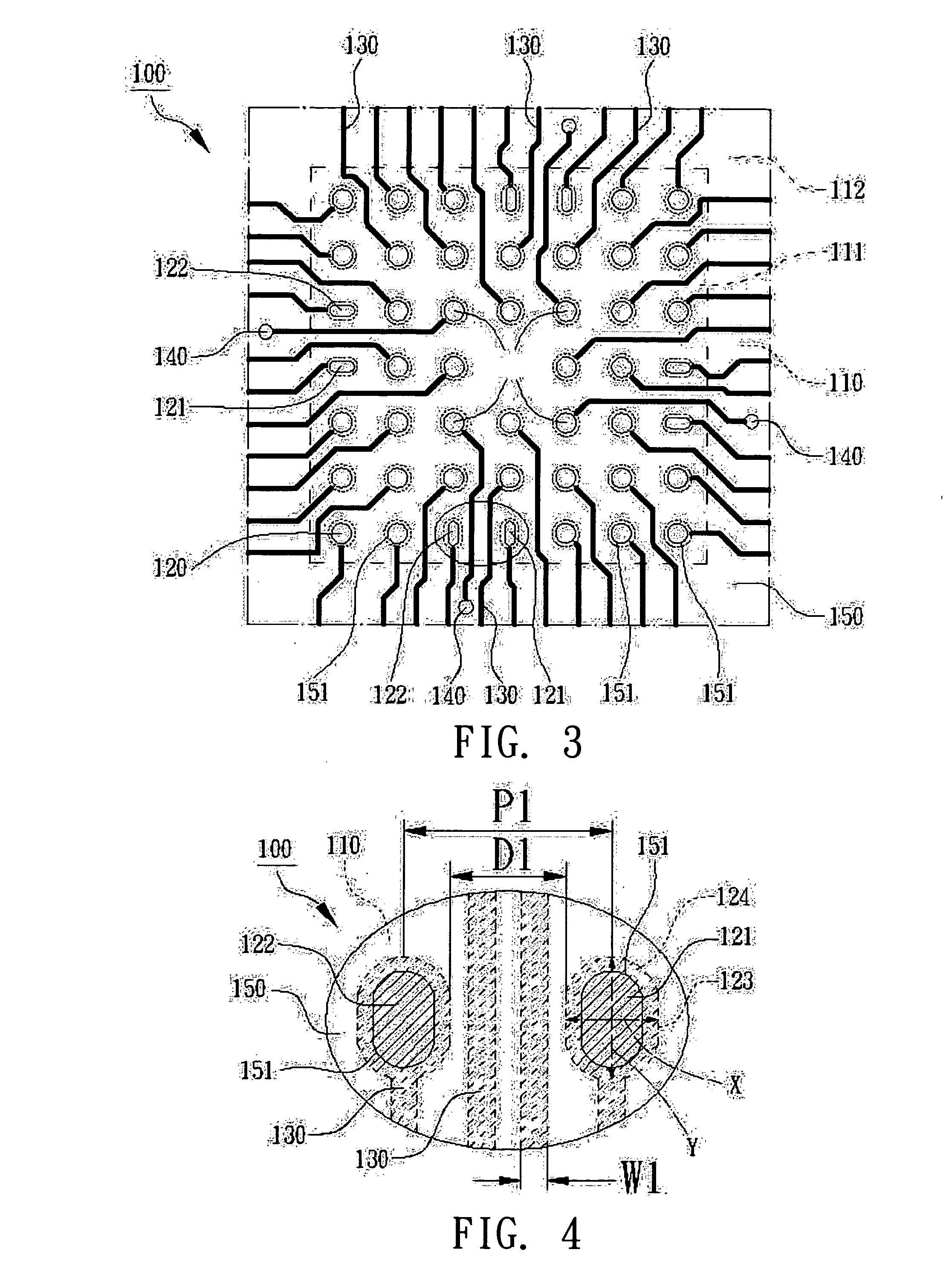
[0016] Referring to FIGS. 3, 4 and 5, a flip-chip package substrate 100 with a high-density layout according to a preferred embodiment of the invention is exemplified. The flip-chip package substrate 100 has an upper surface 110 and a corresponding lower surface 110a. The upper surface 110 is for a flip chip (not shown in the diagram) to be bonded on, the lower surface 110a is a bonding surface of the flip-chip package as shown in FIG. 5. The substrate 100 is a build-up substrate of high-density layout and is preferably made of Bismaleimide Triazine (BT) resin. The substrate 100 can have a number of through holes 140 and a number of metal layers (not shown in the diagram), such as a grounding layer, a power source layer or a signal transmission layer, disposed within for the upper surface 10 and the lower surface 110a of the substrate 100 to be electrically conducted. Referring to FIG. 3, the upper surface 110 of the substrate 100 includes a flip-chip region 111 and a peripheral reg...


PUM


Abstract

A flip-chip package substrate with a high-density layout. A number of pads and a number of traces are formed on an upper surface of the substrate. At least a pad has a short axis and a vertical long axis which are perpendicular to each other. The distance between the elongated pad and the pad adjacent thereto is not smaller than two thirds of the length of the short axis, so that at least two of the traces can pass between the elongated pad and the pad adjacent thereto.

Description

BACKGROUND OF THE INVENTION [0001] 1. Field of the Invention [0002] The invention relates in general to a flip-chip package substrate, and more particularly to a flip-chip package substrate with a high-density layout. [0003] 2. Description of the Related Art [0004] Along with the requirements of slimness, light weight, compactness and high speed, flip-chip package has become the mainstream in semiconductor package. The layout design of the flip-chip package substrate is crucial in meeting the requirements of flip-chip package. The IC chip carrier disclosed in Taiwanese Patent Publication No. 549582 is an example of a flip-chip package substrate according to the prior art. The IC chip carrier includes a substrate, a patterned conducting wire layer and a patterned solder mask. The substrate has an upper surface on which the conducting wire layer and the solder mask are disposed. The conducting wire layer has a number of pads and a number of traces. The pads correspond to a lump on a f...

Claims


Application Information

Patent Timeline
Patent Type & Authority Applications(United States)
IPC IPC(8): H01L21/48H01L23/28H01L23/498H01L23/52
CPCH01L23/49816H01L23/49838H01L2924/0002H01L2924/00H01L2224/81385
Inventor HUNG, CHIH-PINLI, PAO-NANWANG, HSUEH-TETIEN, YUN-HSIANG
Owner ADVANCED SEMICON ENG INC
Why Eureka
Try Eureka