Liquid crystal display device

a liquid crystal display and display device technology, applied in non-linear optics, instruments, optics, etc., can solve the problems of low response speed, deterioration of display quality of lcd devices, and high driving voltage of ush mode lcd devices and blue phase mode lcd devices, so as to reduce driving voltage and improve response speed

Active Publication Date: 2011-06-16
LG DISPLAY CO LTD
View PDF4 Cites 31 Cited by
  • Summary
  • Abstract
  • Description
  • Claims
  • Application Information

AI Technical Summary

Benefits of technology

[0009]An object of the present invention is to provide a liquid crystal display device where a driving voltage is reduced and a respond speed is improved.

Problems solved by technology

Since LCD devices have a low response speed, a display quality of LCD devices is deteriorated due to a residual image.
However, a USH mode LCD device and a blue phase mode LCD device have disadvantages of a high driving voltage.

Method used


Image

  • Liquid crystal display device
  • Liquid crystal display device
  • Liquid crystal display device

Examples


first embodiment

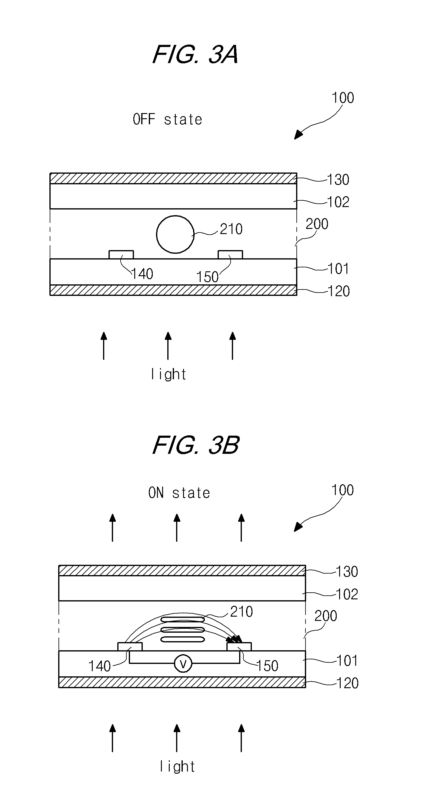
[0044]FIGS. 3A and 3B are cross-sectional views showing OFF and ON states, respectively, of a blue phase mode liquid crystal display device according to the present invention.

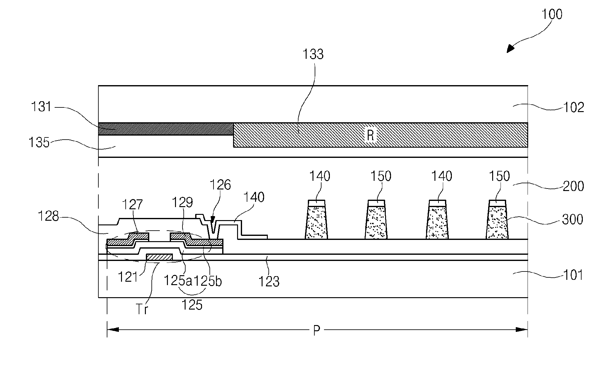
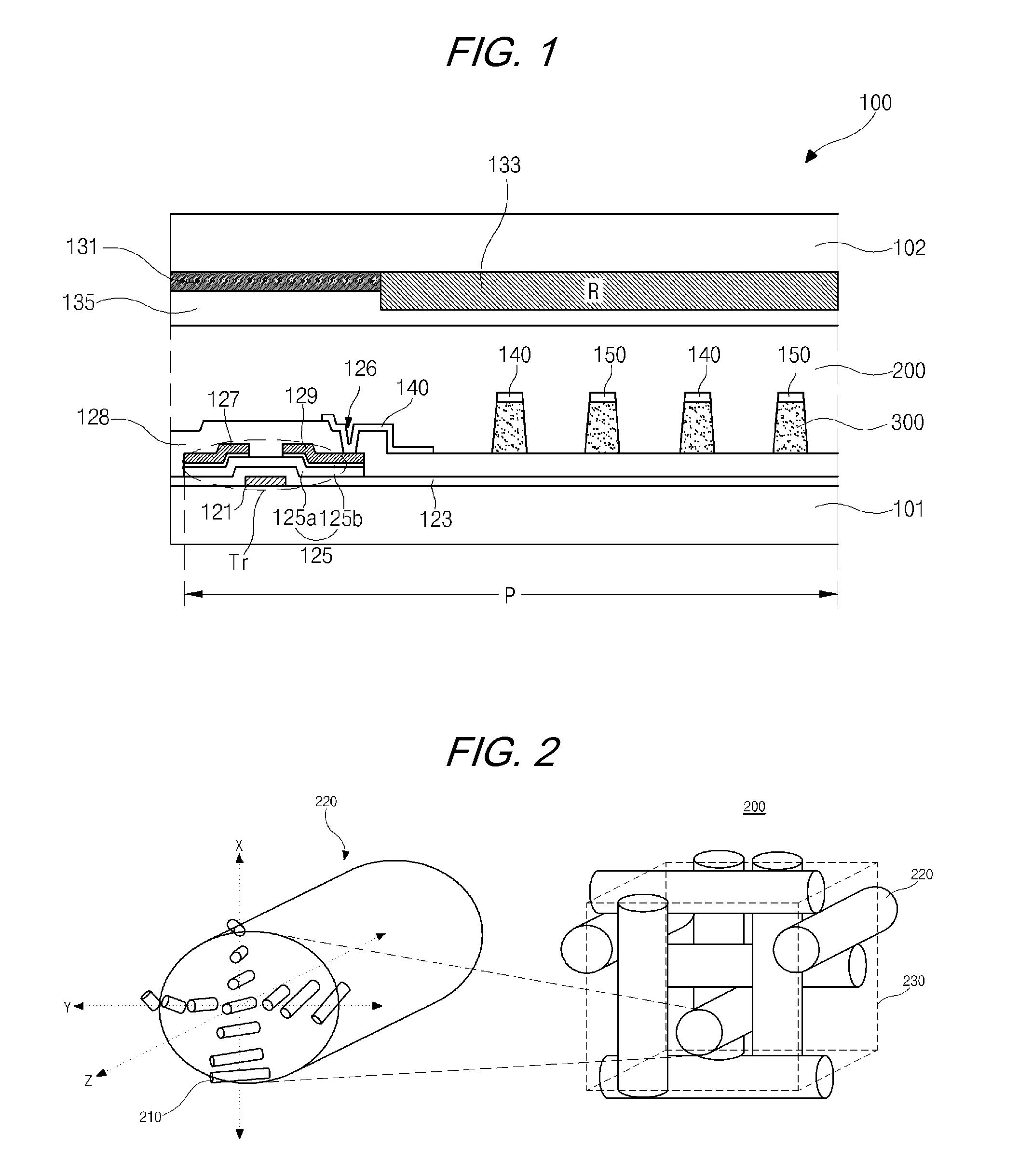
[0045]In FIGS. 3A and 3B, a blue phase mode liquid crystal display (LCD) device 100 includes a liquid crystal panel and a backlight unit (not shown) supplying light to the liquid crystal panel. The liquid crystal panel includes first and second substrates 101 and 102 facing and spaced apart from each other and a blue phase liquid crystal layer 200 between the first and second substrates 101 and 102. A pixel electrode 140 and a common electrode 150 are formed on an inner surface of the first substrate 101. An insulating pattern 300 (of FIG. 1) under each of the pixel electrode 140 and the common electrode 150 is omitted in FIGS. 3A and 3B for illustrating a driving principle. In addition, a first polarizing plate 120 is formed on an outer surface of the first substrate 101, and a second polarizing plate 130 is f...

third embodiment

[0073]FIGS. 8A and 8B are side views showing an OFF state and an ON state, respectively, of a uniform standing helix liquid crystal layer for a liquid crystal display device according to the present invention.

[0074]In FIGS. 8A and 8B, a uniform standing helix (USH) liquid crystal layer 400 includes chiral nematic liquid crystal molecules 410 having a helical structure where the chiral nematic liquid crystal molecules are twisted by several tens times along a helical axis. The chiral nematic liquid crystal molecules 410 having a short pitch are driven by using a flexoelectric effect. In FIG. 8A showing an OFF state of no driving voltage (V=0) (no horizontal electric field), an optic axis is parallel to the helix axis of the chiral nematic liquid crystal molecules 410. In FIG. 8B showing an ON state of a driving voltage (V≠0) (a horizontal electric field), the optic axis rotates to cross the helical axis and the chiral nematic liquid crystal molecules 410 have a birefringence property...


PUM

PropertyMeasurementUnit
thicknessaaaaaaaaaa
thicknessaaaaaaaaaa
thicknessaaaaaaaaaa

Abstract

A liquid crystal display device includes: first and second substrates facing and spaced apart from each other; a plurality of insulating patterns on an inner surface of the first substrate; a plurality of pixel electrodes and a plurality of common electrodes on the plurality of insulating patterns, the plurality of pixel electrodes alternating with the plurality of common electrodes, the adjacent pixel and common electrodes generating a horizontal electric field according to a driving voltage; and a liquid crystal layer between the first and second substrates, the liquid crystal layer including one of a blue phase liquid crystal molecules and a uniform standing helix liquid crystal molecules.

Description

[0001]The present application claims the benefit of Korean Patent Application No. 10-2009-0123495 filed in Korea on Dec. 11, 2009, which is hereby incorporated by reference in its entirety.BACKGROUND OF THE INVENTION[0002]1. Field of the Invention[0003]The present invention relates to a liquid crystal display (LCD) device, and more particularly, to a liquid crystal display device where a driving voltage is reduced due to pixel and common electrodes in a liquid crystal layer.[0004]2. Discussion of the Related Art[0005]As information technology progresses, flat panel display (FPD) devices having light weight, thin profile and low power consumption have been developed. Specifically, a cathode ray tube (CRT) has been replaced by the FPD devices such as a liquid crystal display (LCD) device, a plasma panel display (PDP) device, an electroluminescent display (ELD) device and a field emission display (FED) device.[0006]Among various FPD devices, LCD devices have been widely used for a note...

Claims


Application Information

Patent Timeline
Patent Type & Authority Applications(United States)
IPC IPC(8): G02F1/1333
CPCG02F1/134309G02F1/134363G02F2001/13793G02F1/1418G02F1/1393G02F1/13793G02F1/1343
Inventor LEE, SANG-WOOKPARK, HYUN-JINWOO, JONG-HOONYOON, DONG-KYULEE, WOO-KEUN
Owner LG DISPLAY CO LTD
Why Eureka
Try Eureka