Defect inspection method, and defect inspection device

Inactive Publication Date: 2011-06-16
HITACHI HIGH-TECH CORP
View PDF5 Cites 20 Cited by
  • Summary
  • Abstract
  • Description
  • Claims
  • Application Information

AI Technical Summary

Benefits of technology

[0012]With this invention, the oblique inspection with a high NA and at a low angle of elevation can easily be realized, raisi

Problems solved by technology

In a semiconductor fabrication process, any foreign matters on a substrate to be inspected (wafer) can lead to insulation failures and short-circuits.
Furthermore, as the semiconductor devices are becoming miniaturized, the presence of minute foreign matters can result in insulation failures in capacitors and breakage of gate oxide films and the like.
Similarly in a proc

Method used


Image

  • Defect inspection method, and defect inspection device
  • Defect inspection method, and defect inspection device
  • Defect inspection method, and defect inspection device

Examples


first embodiment

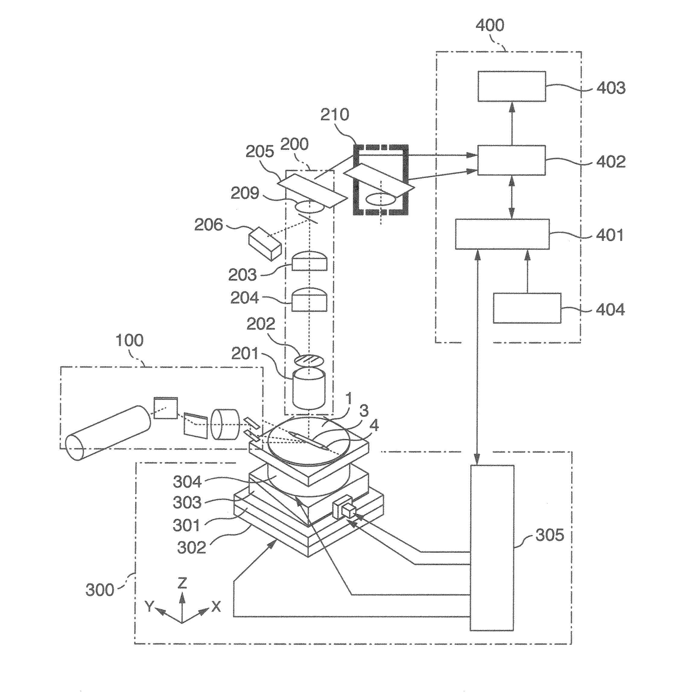
[0054]Referring to FIG. 6, a first embodiment of the oblique inspection according to this invention will be described. An object of this embodiment is to realize a system characterized with an oblique inspection using an overhead detection optic system in order to detect defects on a substrate to be inspected 1 with light.

[0055]A planar reflection mirror 501 is disposed between a detection lens 201 and a substrate to be inspected 1. The planar reflection mirror 501 reflects oblique scattered light obtained from an image sensor detection area 4 on the substrate to be inspected 1. The scattered light reflected by the planar reflection mirror 501 is imaged onto an image sensor 205 by the detection optic system. To this end the reflecting surface of the planar reflection mirror is arranged parallel to a pixel direction (longitudinal direction) of the image sensor and inclined to an optical axis of the detection lens. The detection area 4 of the image sensor does not need to match with t...

second embodiment

[0064]Referring to FIG. 7, a second embodiment of the oblique inspection according to this invention will be explained. The object of this embodiment is to realize a method capable of the overhead inspection and the oblique inspection without changing the stage height as is done in the first embodiment, by setting the stage height of the detection optic system during the overhead inspection and the stage height during the oblique inspection equal or nearly equal and making the focus height of the auto-focus system follow within a pull-in range. For this purpose, it is preferred that an optical path length correction element 503 be disposed between the planar reflection mirror (in this example, a reflecting surface 506 of the optical path length correction element 503) and the detection optic system 200 to extend the optical path length from the inspection area in the substrate to be inspected 1 to the detection lens 201. The optical path length can be extended by as much as (1-1 / ref...

third embodiment

[0067]Referring to FIG. 8, a third embodiment of the oblique inspection according to this invention will be described. The object of this embodiment is to realize a method capable of the overhead inspection and the oblique inspection without changing the stage height by setting the stage height during the overhead inspection and the stage height during the oblique inspection equal using the detection optic system and making the focus height of the auto-focus system follow within a pull-in range. For this purpose, it is desired that an optical path length correction element 504 or 505 be disposed between the planar reflection mirror 501 and the detection optic system 200 to extend the optical path length. The optical path length can be extended by as much as (1-1 / refractive index) times the optical path length passing through the correction element. FIG. 8 shows a construction in which two planar reflection mirrors 501 set at different angles, designed to direct scattered lights with...


PUM


Abstract

Provided are a defect inspection device and a defect inspecting method, which enlarge the uptake range of a light scattered from a fine defect thereby to heighten signal intensity. The defect inspection device is provided with: a stage unit (300) capable of mounting an inspection object substrate (1) thereon to move same relative to an optical device; an illuminating optical device (100) for illuminating an inspection zone (4) on the inspection object substrate (1); a detecting optical device (200) for detecting a light from the inspection zone (4) of the inspection object substrate (1); an image sensor (205) for converting the image focused by the detecting optical device (200) into signals; a signal processing unit (402) for processing the signals from the image sensor (205) thereby to detect a defect; and a plane reflecting mirror (501) arranged between detecting optical device (200) and the inspection object substrate (1) and transmitting the light from the inspection object substrate (1) to the detecting optical device (200).

Description

TECHNICAL FIELD [0001]The present invention relates to a defect inspection method and a defect inspection device and particularly to a technology suited for inspecting the situation of generation of defects such as foreign matters in a fabrication process in which defects such as foreign matters generated during the process are detected and analyzed to take measures during those processes in which object devices are produced by forming a pattern on a substrate, including a semiconductor fabrication process, a liquid crystal display element fabrication process, and a printed circuit board fabrication process.BACKGROUND ART [0002]In a semiconductor fabrication process, any foreign matters on a substrate to be inspected (wafer) can lead to insulation failures and short-circuits. Furthermore, as the semiconductor devices are becoming miniaturized, the presence of minute foreign matters can result in insulation failures in capacitors and breakage of gate oxide films and the like. These f...

Claims


Application Information

Patent Timeline
IPC IPC(8): G01N21/956
CPCG01N21/956
Inventor CHIKAMATSU, SHUICHINOGUCHI, MINORUOCHI, MASAYUKIAIKO, KENJI
Owner HITACHI HIGH-TECH CORP
Why Eureka
Try Eureka