
Substrate metallization and ball attach metallurgy with a novel dopant element

a technology of dopant elements and substrate metallurgy, which is applied in the direction of printed circuit details, printed circuit manufacture, circuit packaging, etc., can solve the problems of insufficient flux time, solder ball failure to properly adhere to the surface of the board, and circuit package warpage of various degrees

Inactive Publication Date: 2011-06-23
INTEL CORP
View PDF21 Cites 6 Cited by
  • Summary
  • Abstract
  • Description
  • Claims
  • Application Information

AI Technical Summary

Problems solved by technology

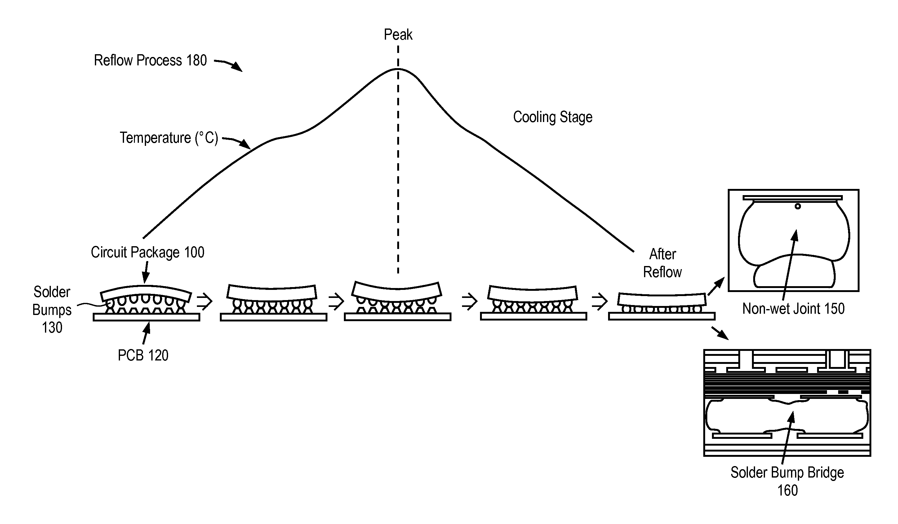
During the reflow process, circuit packages often experience various degrees of warpage as the temperature changes.
The changing degrees of warpage can be referred to as “dynamic warpage.” Dynamic warpage is often the cause of non-wet joints, which means the solder balls fail to properly adhere to the surface of the board.
For example, during the surface mount (SMT) reflow, dynamic warpage usually results in insufficient time for the flux to clean off the oxide and residue layer on the solder balls to form proper solder joints.
Further, dynamic warpage can result in an inadequate flux and solder ball contact.
The inadequate flux and solder ball contact can cause non-uniform collapse of the solder balls during the reflow.
Solder bump bridging may be the cause of a short circuit.
During the reflow, mismatch in thermal expansions causes circuit package 100 to warp.
The non-wet joint and solder bump bridging can result in failures of the circuit package or the board.
However, the conventional solutions have had minimal success, with an increased risk for other issues, such as solder bridging.

Method used


Image

  • Substrate metallization and ball attach metallurgy with a novel dopant element
  • Substrate metallization and ball attach metallurgy with a novel dopant element
  • Substrate metallization and ball attach metallurgy with a novel dopant element

Examples


Embodiment Construction

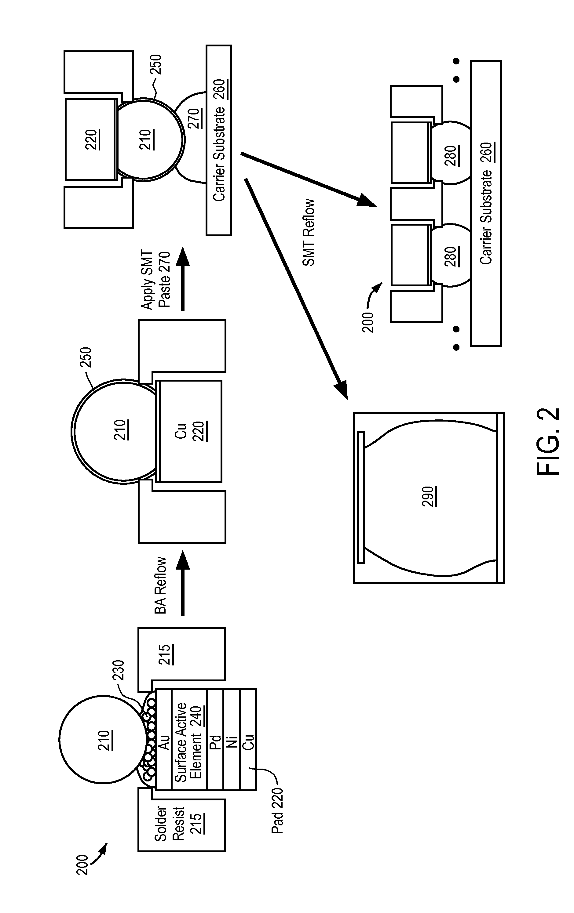
FIG. 2 shows a cross-sectional view of a portion of a circuit package 200 that includes a conductive element (e.g., a solder element 210) and a region adjacent to and to be bonded with solder element 210. Solder element 210 may be formed by tin (Sn) based material, Indium (In) based material, or other suitable solder materials. Although one solder element 210 is shown, it is understood that circuit package 200 may include an array or a matrix of solder elements for forming an electrical and mechanical connection with a carrier substrate, such as a printed circuit board (PCB) or another component package. The region of circuit package 200 adjacent to, and to be bonded with, solder element 210 includes a pad 220 within the substrate of circuit package 200 (referred to as the package substrate) and a bonding material (e.g., solder paste 230) applied on top of pad 220. Pad 220 may include a number of metal layers (e.g., a copper (Cu) layer, a nickel (Ni) layer, a palladium (Pd) layer an...


PUM

PropertyMeasurementUnit
Surfaceaaaaaaaaaa
Wetting tensionaaaaaaaaaa

Abstract

Surface-active dopants are added to a portion of a circuit package before a reflow process to promote wetting and reduce the formation of solder bump bridges. The circuit package has a solder element that electrically connects the circuit package to a substrate. A reflow process is performed to attach the solder element to a pad on the circuit package. During the reflow process, the surface-active dopants diffuse to the surface of the solder element and form an oxide passivation layer on the surface of the solder element.

Description

BACKGROUND1. FieldTechnology for interconnecting integrated circuitry, packages and printed circuit boards.2. BackgroundIn metallurgy, “wetting” refers to the ability of a liquid to maintain contact with a solid surface. Wetting is an important factor in bonding two materials. When bonding a circuit package with a carrier (e.g., a printed circuit board), solder paste may be used to temporarily hold the solder balls (or solder bumps) on the circuit package to the board. A reflow process can be performed to melt the solder balls (or solder bumps), which form solder joints after the molten solder is cooled. The solder joints provide an electrical and mechanical connection between the package and the board.During the reflow process, circuit packages often experience various degrees of warpage as the temperature changes. The changing degrees of warpage can be referred to as “dynamic warpage.” Dynamic warpage is often the cause of non-wet joints, which means the solder balls fail to prope...

Claims


Application Information

Patent Timeline
IPC IPC(8): H05K1/11H01R9/00
CPCY10T29/49144H05K3/3489Y10T29/49149H05K3/3436Y10T29/49213
Inventor SIDHU, RAJEN S.DANI, ASHAY A.RENAVIKAR, MUKUL P.
Owner INTEL CORP
Learn More