Module for Use in a Multi Package Assembly and a Method of Making the Module and the Multi Package Assembly

Inactive Publication Date: 2011-06-23
HONG KONG APPLIED SCI & TECH RES INST
View PDF24 Cites 10 Cited by
  • Summary
  • Abstract
  • Description
  • Claims
  • Application Information

AI Technical Summary

Benefits of technology

[0014]As the lower module has a second substrate with electrical connectors on either side, the stand off height may be increased. Further, the opening in the second substrate makes room for one or more chips mounted to the first substrate. Overmolded means that molding material covers the second substrate. As the ‘intermediate’ second substrate and the second connectors are overmolded, the assembly is less prone to warpage. Preferably the at least one chip is overmolded. Preferably the first substrate is overmolded. Preferably the overmold extends over the first substrate at least as far as the second substrate; more preferably the whole of the first substrate is overmolded. The assembly is also relatively cheap to manufacture compared to other arrangements which require laser drilling or other complex machinery.
[0015]Preferably there are a plurality of first ele

Problems solved by technology

Firstly as electronic devices increase in complexity it is necessary to increase the density of connections, which requires very fine pitch of connectors.
This is difficult to achieve.
Secondly, the

Method used


Image

  • Module for Use in a Multi Package Assembly and a Method of Making the Module and the Multi Package Assembly
  • Module for Use in a Multi Package Assembly and a Method of Making the Module and the Multi Package Assembly
  • Module for Use in a Multi Package Assembly and a Method of Making the Module and the Multi Package Assembly

Examples


Embodiment Construction

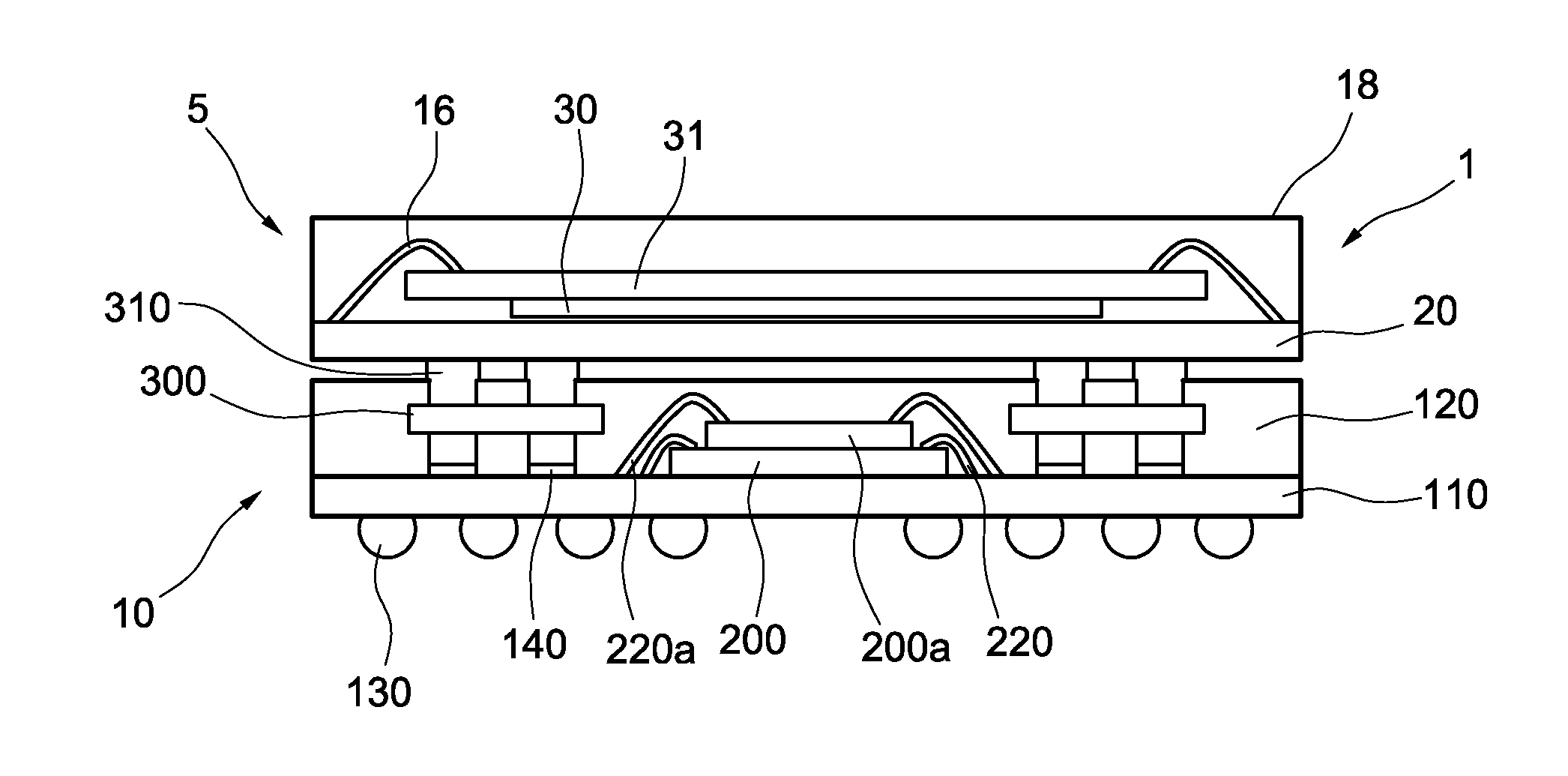
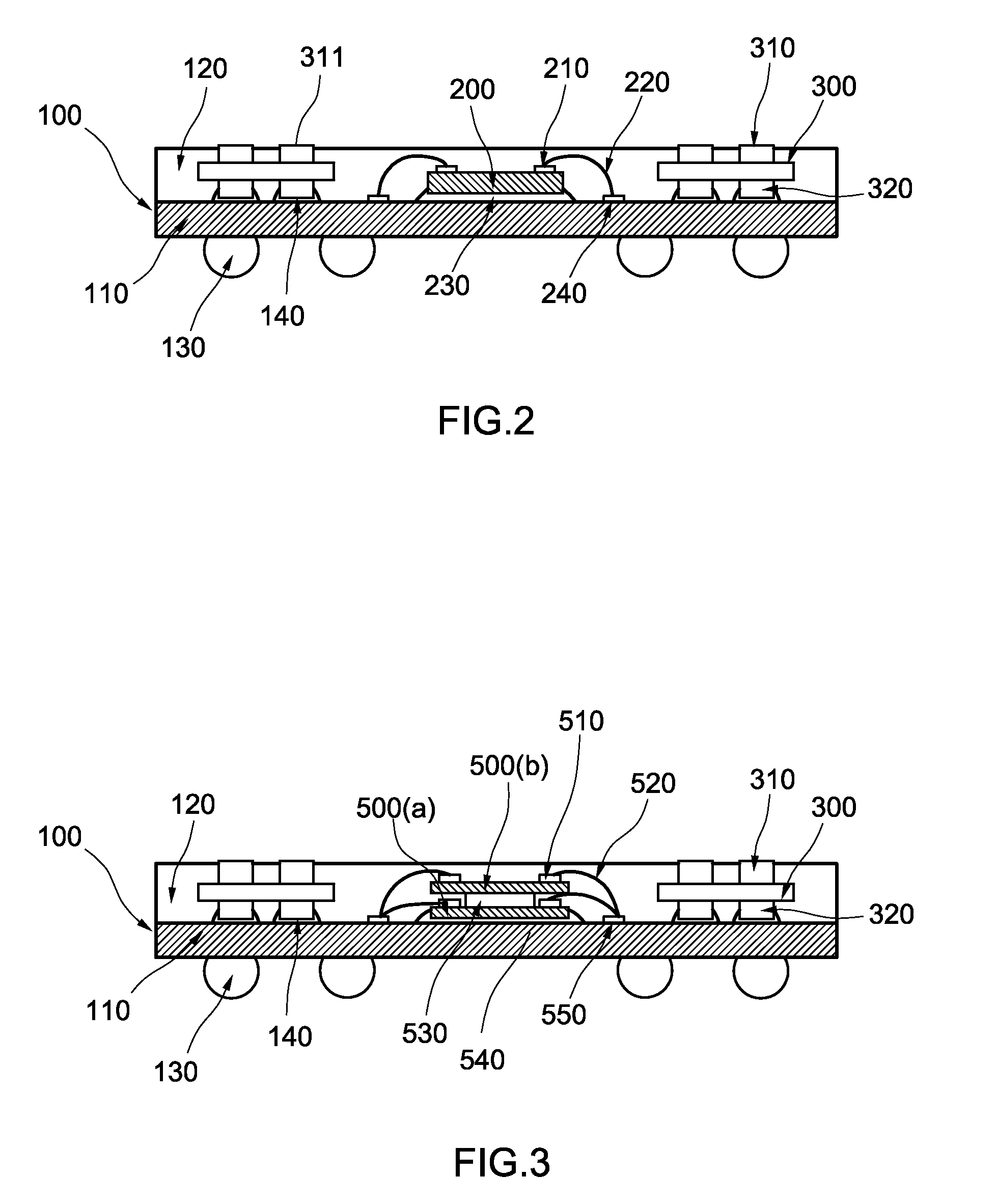
[0047]FIG. 2 shows a module 100 for use in a multichip package. In particular a module for use in the lower part of a PoP assembly. It comprises a first substrate 110 which maybe a PCB, preferably a BT core substrate. A (bismaleimide triazine) core substrate, is a substrate comprising a BT core layer with a metal layer on either side. BT has the advantage that it is a polymide with higher thermal stability, better chemical resistance and mechanical properties compared to the expoxy resin used in same other types of PCB. Solder balls 130 are provided on the lower side of the first substrate 110 to enable the module 100 to be mounted to an external apparatus, such as a motherboard. A chip 200, which may be a memory chip or a processor, is mounted to the first substrate 100. It may be mounted by any appropriate method, for example die attachment with wire bonding, flip chip etc. Wires 220 connect a bonding pad 210 on top of the chip 200 with a bonding pad 240 on the upper side of the f...


PUM


Abstract

The module comprises a first substrate and at least one chip mounted on the first substrate. A second substrate is mounted to the first substrate and has an opening therein. The opening is lined with the at least one chip. The second substrate is overmolded and the first substrate is electrically connected to the second substrate by at least one first electrical connector. At least one second electrical connector extends from the second substrate through the overmold and has its exposed ends for electrical connection to an external module. The external module may be mounted to the first module in order to form a package on package assembly.

Description

TECHNICAL FIELD[0001]The present invention relates to package on package (PoP) technology. In particular it relates to a module for use in a multi-package assembly and a method of making the module and a multi-package assembly.BACKGROUND OF THE INVENTION[0002]A package on package (PoP) comprises two electronic packages assembled in a vertical stack. It may use a variety of package styles, but fine-pitch ball grid array (FBGA) is the most common.[0003]A typical PoP assembly 1 is shown in FIG. 1. It comprises a first electronic package 5 mounted on top of a second electronic package 10. Typically the top package 5 has a memory device, while the bottom package has a processor.[0004]Due to their compact nature, PoP assemblies are used in many electronic devices. For example in a mobile phone the top package may have a memory device and the bottom package a baseband or applications processor. In a digital camera the top package may have a memory device and the bottom package an image pro...

Claims


Application Information

Patent Timeline
IPC IPC(8): H01L23/52H01L21/60
CPCH01L24/48H01L2225/1023H01L2924/15311H01L2924/3511H01L24/83H01L25/105H01L2224/83H01L23/49816H01L2225/1041H01L2924/01327H01L21/56H01L2224/32145H01L2224/85H01L2224/73265H01L2224/32225H01L2225/1058H01L2224/48227H01L23/3128H01L2924/15331H01L24/85H01L23/49833H01L2924/19041H01L2924/3512H01L2924/00H01L2924/00012H01L24/73H01L2924/181H01L2924/00014H01L2224/45099H01L2224/45015H01L2924/207
Inventor SUN, PENGLEUNG, CHI KUEN VINCENTSHI, XUN QING
Owner HONG KONG APPLIED SCI & TECH RES INST
Why Eureka
Try Eureka