Touch panel and fabricating method thereof

a technology of capacitive touch panel and manufacturing method, which is applied in the field of touch panel, can solve the problems of high manufacturing cost and high manufacturing process cost, and achieve the effect of reducing manufacturing cos

Active Publication Date: 2011-06-23
AU OPTRONICS CORP
View PDF8 Cites 54 Cited by
  • Summary
  • Abstract
  • Description
  • Claims
  • Application Information

AI Technical Summary

Benefits of technology

[0009]Since the method of fabricating the touch panel in accordance with the present invention utilizes screen printing processes to define both a patterned sacrificial layer of the patterned sensing pad layer and a patterned sacrificial layer of the patterned bridge line layer, the method of fabricating the touch panel in accordance with the present invention can greatly reduce the manufacturing cost in comparison to the conventional method which uses a photolithography process.

Problems solved by technology

The sensing pads, and the film layers such as the insulating layer and the bridge line of the conventional capacitive touch panels are respectively formed using a photolithography process, so that the manufacturing process is expensive and the high manufacturing cost ultimately affects the popularity of the capacitive touch panels.

Method used


Image

  • Touch panel and fabricating method thereof
  • Touch panel and fabricating method thereof
  • Touch panel and fabricating method thereof

Examples


Embodiment Construction

[0015]To provide a better understanding of the present invention, preferred embodiments will be detailed as follows. The preferred embodiments of the present invention are illustrated in the accompanying drawings with numbered elements to elaborate the contents and effects to be achieved. Furthermore, the terms “first”, “second”, “third” and “fourth” are used to distinguish between different devices or processes, and do not limit the sequence of the devices or processes.

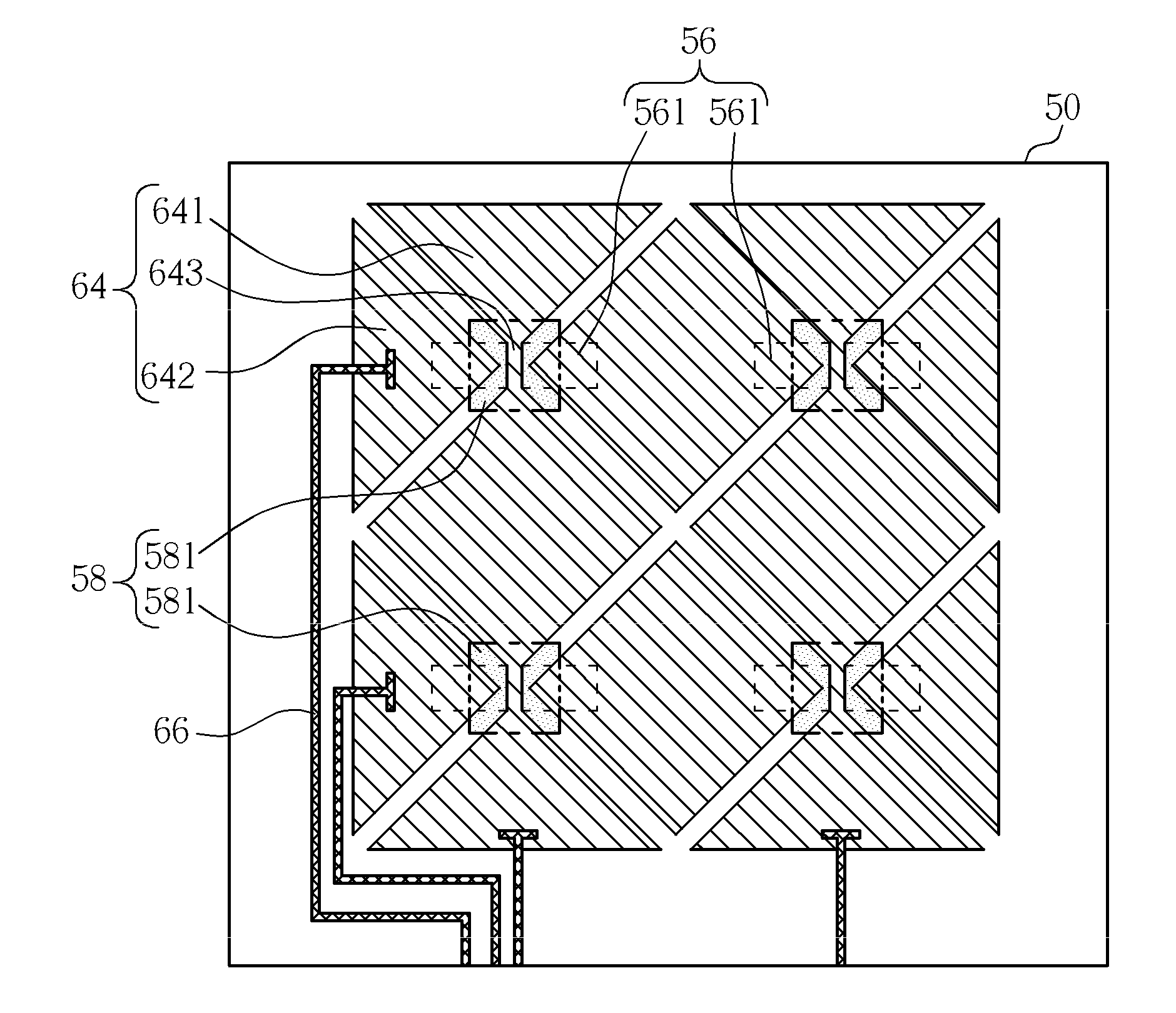
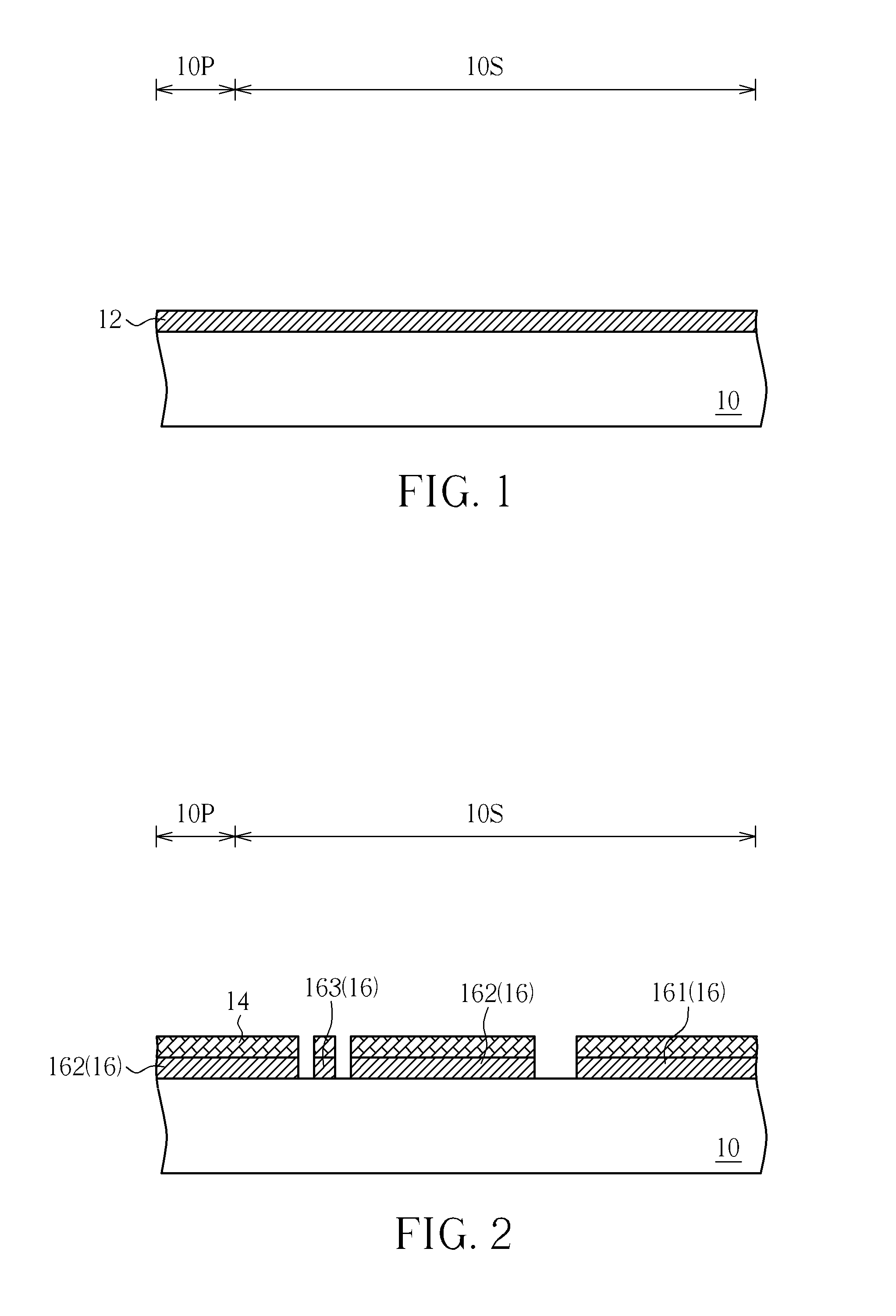
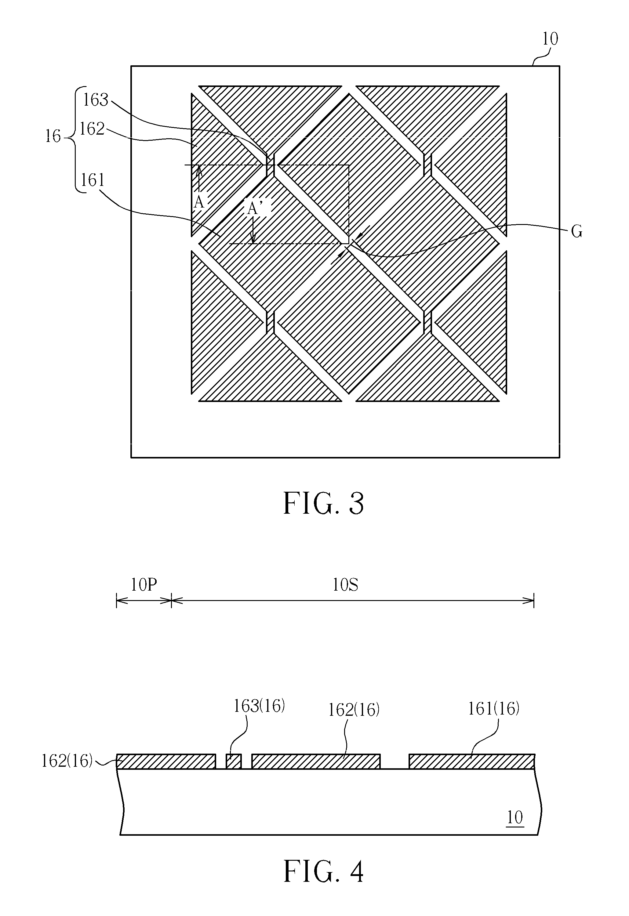
[0016]Referring to FIG. 1 to FIG. 9, FIG. 1 to FIG. 9 are schematic diagrams illustrating a method of fabricating a touch panel in accordance with a first embodiment of the present invention. To better illustrate the characteristics of the present invention, FIG. 3 and FIG. 8 are top view diagrams, and FIG. 1, FIG. 2, FIG. 4 to FIG. 7 and FIG. 9 are cross-sectional diagrams across line A-A′ of FIG. 3. As illustrated in FIG. 1, a base 10 is first provided, and the base 10 at least includes a sensing region 10S for dis...


PUM

PropertyMeasurementUnit
widthaaaaaaaaaa
widthaaaaaaaaaa
thicknessaaaaaaaaaa

Abstract

A method of fabricating touch panel includes the following steps. A base is provided. A first transparent conductive layer is formed on the base. A first screen printing process is performed to form a first patterned sacrificial layer on the first transparent conductive layer, and the first patterned sacrificial layer is used to pattern the first transparent conductive layer to form a patterned sensing pad layer. A second screen printing process is carried out to form a patterned insulating layer. A second transparent conductive layer is formed on the base. A third screen printing process is performed to form a second patterned sacrificial layer, and the second patterned sacrificial layer is used to pattern the second transparent conductive layer to form a patterned bridge line layer.

Description

BACKGROUND OF THE INVENTION[0001]1. Field of the Invention[0002]The present invention relates to a touch panel and a fabricating method thereof, and more particularly to a touch panel and a fabricating method thereof utilizing screen printing processes to form a patterned sensing pad layer, a patterned insulating layer, and a patterned bridge line layer of the touch panel.[0003]2. Description of the Prior Art[0004]In the present consumer electronic product market, touch panels have been widely applied in portable electronic products such as mobile phone, global positioning system (GPS), digital media player, and the touch panels act as human machine interface (HMI). Since the demands of the present consumer electronic products tend to be light in weight, thin in profile and short in size, the idea of replacing the conventional input devices such as keyboard and mouse with the touch panels could effectively reduce the size of the electronic devices; therefore, the touch panels have b...

Claims


Application Information

Patent Timeline
Patent Type & Authority Applications(United States)
IPC IPC(8): G06F3/041H05K3/00
CPCH05K2203/0568Y10T29/49124G06F2203/04103G06F2203/04111G06F3/044H05K2201/0326H05K3/4685H05K3/061G06F3/0446
Inventor LU, YING-CHIHUANG, SHU-HUICHOU, SHIH-POLEE, SEOK-LYUL
Owner AU OPTRONICS CORP
Why Eureka
Try Eureka