Liquid crystal display device and driving method thereof

a technology of liquid crystal display device and driving method, which is applied in the direction of semiconductor devices, instruments, computing, etc., can solve the problems of reducing display quality, affecting the display quality, and reducing the power consumption of the liquid crystal display device, so as to suppress the deterioration of display quality and reduce the power consumption

Active Publication Date: 2011-06-23
SEMICON ENERGY LAB CO LTD
View PDF101 Cites 84 Cited by
  • Summary
  • Abstract
  • Description
  • Claims
  • Application Information

AI Technical Summary

Benefits of technology

[0015]According to one embodiment of the present invention, power consumption in the case where a still image is displayed on a liquid crystal display device can be reduced. Further, according to one embodiment of the present invention, deterioration of the display quality can be suppressed.

Problems solved by technology

However, in the above-referenced driving methods, a configuration of a driver circuit which supplies a signal to a scan line or a signal line of the liquid crystal display device and an operation thereof are complicated, so that power consumption of the liquid crystal display device cannot be reduced enough.
Large decrease in the voltage applied to the liquid crystal element lowers display quality; for example, display with a predetermined gray scale level cannot be performed.

Method used


Image

  • Liquid crystal display device and driving method thereof
  • Liquid crystal display device and driving method thereof
  • Liquid crystal display device and driving method thereof

Examples


embodiment 1

[0032]In Embodiment 1, a driving method of a liquid crystal display device according to one embodiment of the present invention and the liquid crystal display device will be described.

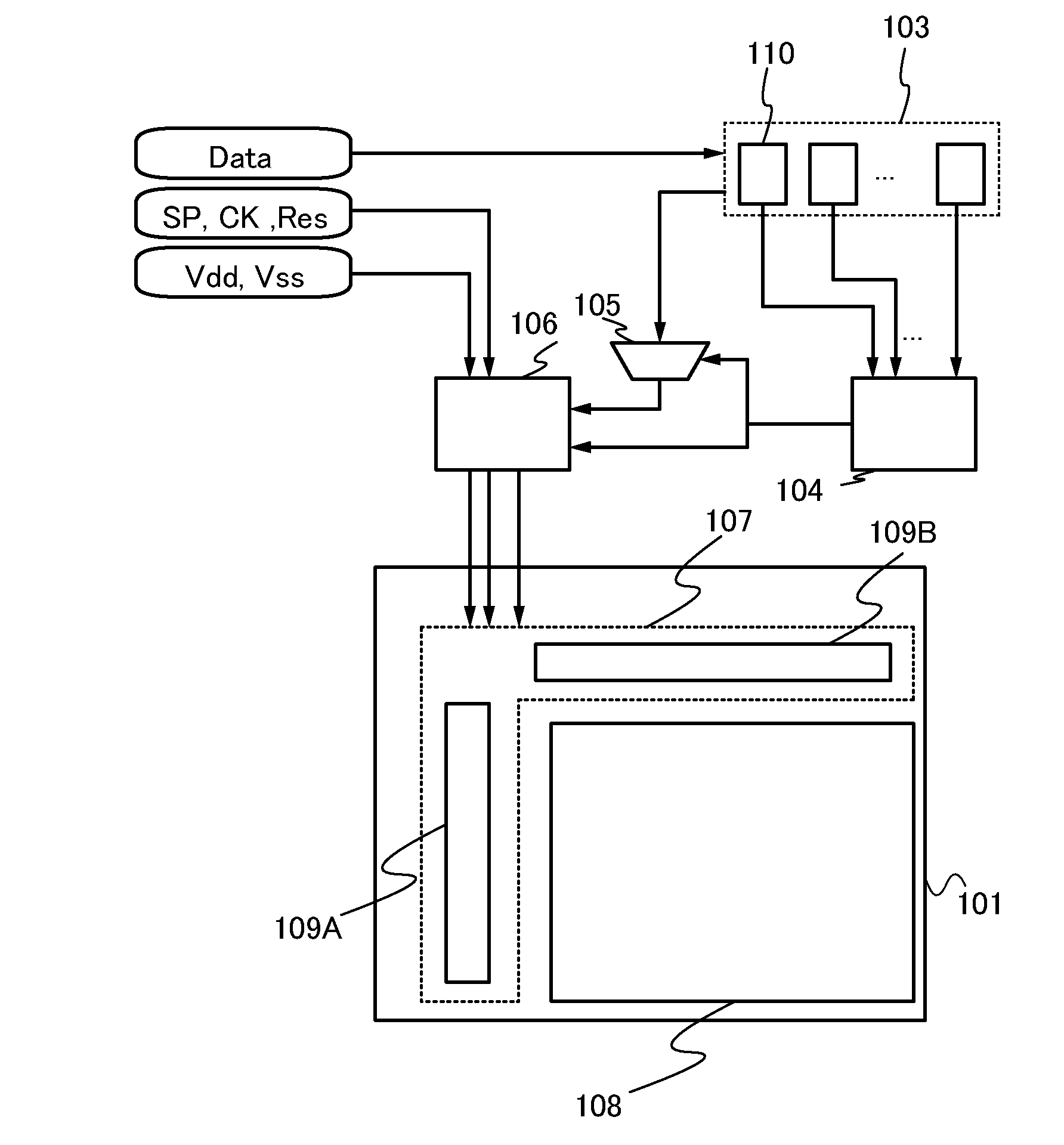
[0033]First, a structure of the liquid crystal display device in this embodiment is described with reference to FIG. 1. FIG. 1 is a block diagram illustrating an example of the structure of the liquid crystal display device in this embodiment.

[0034]A liquid crystal display device shown in FIG. 1 includes a display panel 101, a memory circuit 103, a comparison circuit 104, a selection circuit 105, and a display control circuit 106.

[0035]The display panel 101 includes a driver circuit portion 107 and a pixel portion 108.

[0036]The driver circuit portion 107 includes a driver circuit 109A and a driver circuit 109B. The pixel portion 108 includes a plurality of pixels. The driver circuits 109A and 109B are driver circuits for driving the plurality of pixels in the pixel portion 108. The driver circuit 109A ...

embodiment 2

[0092]In Embodiment 2, a structure of a shift register included in each of a scan line driver circuit and a signal line driver circuit of the liquid crystal display device described in Embodiment 1 will be described.

[0093]An example of the structure of the shift register in this embodiment is described with reference to FIGS. 5A to 5C. FIGS. 5A to 5C are diagrams illustrating an example of the structure of the shift register in this embodiment.

[0094]A shift register shown in FIG. 5A includes first to N-th pulse output circuits 10_1 to 10_N (N is a natural number greater than or equal to 3).

[0095]Each of the first to N-th pulse output circuits 10_1 to 10_N is electrically connected to three wirings among first to fourth wirings 11 to 14. In the shift register shown in FIG. 5A, a first clock signal CK1 is supplied through the first wiring 11, a second clock signal CK2 is supplied through the second wiring 12, a third clock signal CK3 is supplied through the third wiring 13, and a four...

embodiment 3

[0126]In Embodiment 3, an example of a transistor which is applicable as the transistor included in the liquid crystal display device described in Embodiment 1 will be described.

[0127]A transistor in this embodiment is described below with reference to FIGS. 8A to 8D. FIGS. 8A to 8D are views for illustrating the transistor described in Embodiment 1.

[0128]A process for manufacturing a transistor 410 over a substrate 400 is described below with reference to FIGS. 8A to 8D.

[0129]First, a conductive film is formed over the substrate 400 having an insulating surface, a resist mask is formed over the conductive film by a first photolithography process, and then, the conductive film is etched using the resist mask, so that a gate electrode layer 411 is formed. After that, the resist mask is removed. The resist mask may be formed by an inkjet method. Formation of a resist mask by an inkjet method does not use a photomask, so that the manufacturing cost can be reduced.

[0130]Although there i...


PUM


Abstract

Disclosed is a liquid crystal display device and a driving method thereof for displaying an image, in which the polarity of a voltage applied to the liquid crystal element is inverted in a first frame period and a second frame period which are sequential. The voltage applied to the liquid crystal element is compensated in the case where images of the first frame period and the second frame period are judged as a still image as a result of comparison of the image of the first frame period with the image of the second frame period and the absolute value of the voltage applied to the liquid crystal element in the first frame period is different from that of the voltage applied to the liquid crystal element in the second frame period.

Description

TECHNICAL FIELD[0001]The present invention relates to a liquid crystal display device and a method for driving the liquid crystal display device.BACKGROUND ART[0002]Liquid crystal display devices have been applied in a wide range of fields from large display devices such as TV sets to small display devices such as mobile phones, and those with higher added value have been developed. In recent years, in view of rising interest in the global environment and improvement of the convenience of mobile devices, development of liquid crystal display devices with low power consumption has attracted attention.[0003]For example, Patent Document 1 discloses a technique for reducing the power consumption of a liquid crystal display device, according to which all of the signal lines are electrically disconnected to a signal line driver circuit to have high impedance in order to keep the voltage of each signal line constant in a break period during which no scan line and no signal line are selecte...

Claims


Application Information

Patent Timeline
Patent Type & Authority Applications(United States)
IPC IPC(8): G09G5/00G09G3/36
CPCG09G3/3614G09G2320/0247G09G2320/103G09G3/3696G09G2340/16H01L27/1225G09G2330/021
Inventor ARASAWA, RYOTOYOTAKA, KOUHEI
Owner SEMICON ENERGY LAB CO LTD
Why Eureka
Try Eureka