Pixel structure and display panel

a pixel structure and display panel technology, applied in the field of pixel structure and display panel, can solve the problems of poor display quality of the lcd panel, insufficient anchoring energy on the alignment surface, etc., and achieve the effect of reducing the generated display mura

Active Publication Date: 2011-06-23
AU OPTRONICS CORP
View PDF6 Cites 31 Cited by
  • Summary
  • Abstract
  • Description
  • Claims
  • Application Information

AI Technical Summary

Benefits of technology

[0009]The present invention is directed to a pixel structure and a display panel having the same, which are capab

Problems solved by technology

Though the non-contact alignment process solves the problems of electrostatics and particle contamination in the contact friction alignment, it often leads to the pr

Method used


Image

  • Pixel structure and display panel
  • Pixel structure and display panel
  • Pixel structure and display panel

Examples


Embodiment Construction

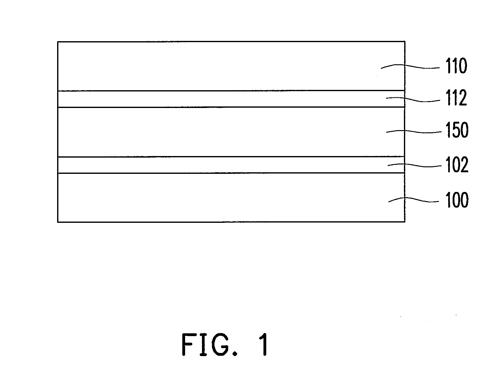
[0025]FIG. 1 is a schematic cross-sectional view of a display panel according to an embodiment of the present invention. Referring to FIG. 1, the display panel of the present embodiment includes a first substrate 100, a second substrate 110, and a display medium 150 between the first substrate 100 and the second substrate 110.

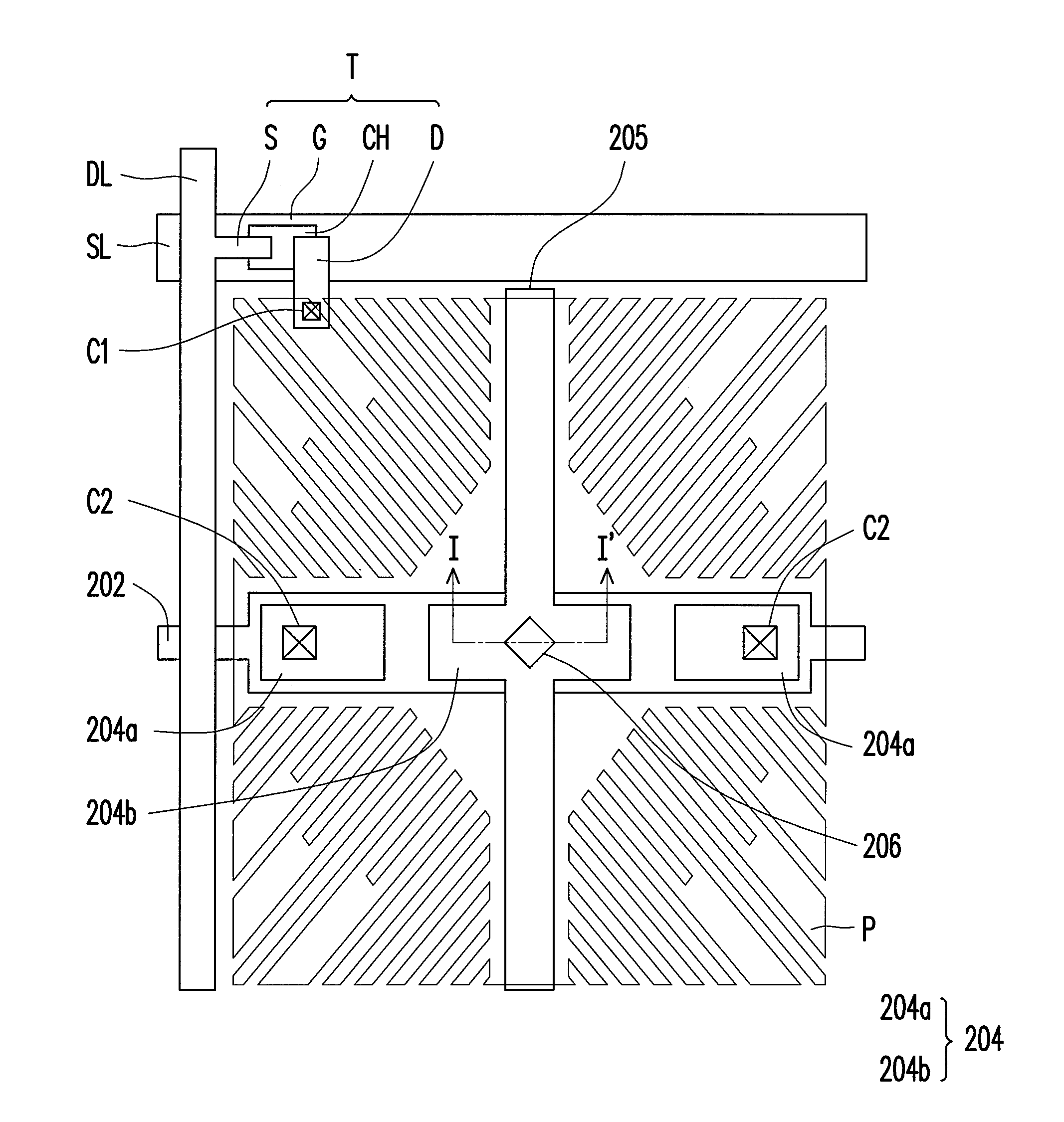
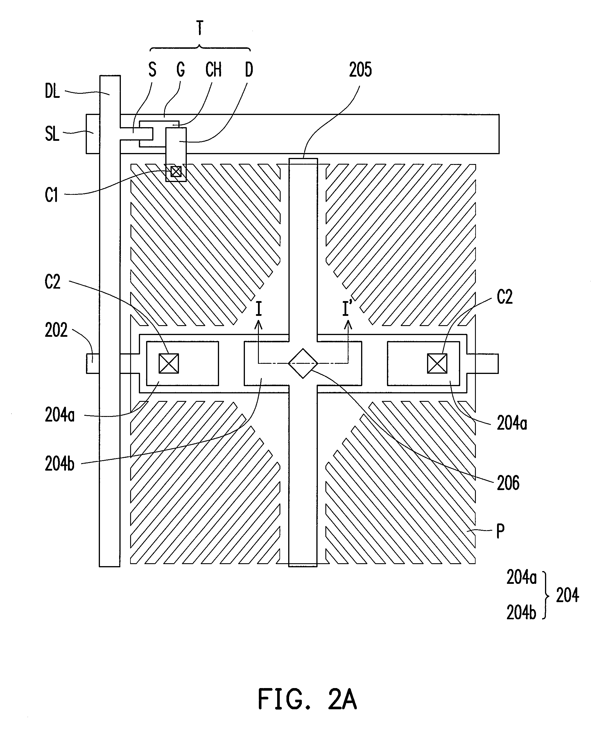
[0026]The first substrate 100 can be made of glass, quartz, an organic material or a metal. The first substrate 100 has a pixel array layer 102 thereon, and the pixel array layer 102 includes a plurality of pixel structures. The pixel structures of the pixel array layer 102 are described in the subsequent paragraphs.

[0027]The second substrate 110 can be made of glass, quartz, an organic material or the like. An electrode layer 112 is disposed on the second substrate 110. In the embodiment, the electrode layer 112 is a transparent electrode layer and can be, for example, made of indium tin oxide (ITO) or indium zinc oxide (IZO). The electrode layer 112 completel...


PUM

PropertyMeasurementUnit
Thicknessaaaaaaaaaa
Structureaaaaaaaaaa
Lengthaaaaaaaaaa

Abstract

A pixel structure including a substrate, a scan line, a data line, an active device, a capacitor electrode line, an upper electrode pattern and a pixel electrode is described. The scan line and the data line are disposed on the substrate. The active device is electrically connected to the scan line and the data line. The capacitor electrode is disposed on the substrate. The upper electrode pattern is disposed above the capacitor electrode line, and the upper electrode pattern has a first opening therein to expose the capacitor electrode pattern. The pixel electrode is electrically connected with the active device and covers the capacitor electrode line and the upper electrode pattern, wherein the pixel electrode has a middle portion and a plurality of branches connecting to the middle portion, and the middle portion has a second opening therein to expose the first opening.

Description

CROSS-REFERENCE TO RELATED APPLICATION[0001]This application claims the priority benefit of Taiwan application serial no. 98144320, filed on Dec. 22, 2009. The entirety of the above-mentioned patent application is hereby incorporated by reference herein and made a part of specification.BACKGROUND OF THE INVENTION[0002]1. Field of the Invention[0003]The present invention relates to a pixel structure and a display panel having the same, and particularly to a pixel structure and a display panel having the same using polymer stabilized alignment (PSA) technique.[0004]2. Description of Related Art[0005]In the development of the display, with the progress in the optoelectronic techniques and the semiconductor manufacturing techniques, the liquid crystal display with the advantages of high definition, optimal space utilization, low power consumption, and no radiation has gradually become the main stream of the market.[0006]A liquid crystal display includes a backlight module and a liquid c...

Claims


Application Information

Patent Timeline
IPC IPC(8): G02F1/1343
CPCG02F1/133707G02F1/133711G02F2001/136218G02F2001/133757G02F2001/133776G02F1/136213G02F1/133757G02F1/133776G02F1/136218
Inventor TSAO, CHENG-HANCHO, TING-YICHIU, CHUNG-YI
Owner AU OPTRONICS CORP
Why Eureka
Try Eureka