Semiconductor device

a technology of semiconductors and semiconductors, applied in the direction of digital storage, capacitors, instruments, etc., can solve the problems of long time-consuming data storage, achieve the effect of reducing power consumption, ensuring data integrity, and ensuring data integrity

Active Publication Date: 2011-06-30
SEMICON ENERGY LAB CO LTD
View PDF99 Cites 224 Cited by
  • Summary
  • Abstract
  • Description
  • Claims
  • Application Information

AI Technical Summary

Benefits of technology

[0022]Since the off current of a transistor using an oxide semiconductor is extremely low, stored data can be stored for an extremely long time by using the transistor. In other words, power consumption can be considerably reduced because refresh operation becomes unnecessary or the frequency of refresh operation can be extremely low. Moreover, stored data can be stored for a long time even when power is not supplied.
[0023]Further, a semiconductor device according to one embodiment of the disclosed invention does not need high voltage for writing of data and there is no problem of deterioration of elements. For example, since there is no need to perform injection of electrons to a floating gate and extraction of electrons from the floating gate which are needed in a conventional nonvolatile memory, deterioration of a gate insulating layer does not occur. In other words, one embodiment of the semiconductor device according to the present invention does not have a limit on the number of times of writing which is a problem in a conventional nonvolatile memory, and reliability thereof is drastically improved. Furthermore, data is written depending on on and off of the transistor, whereby high-speed operation can be easily realized. In addition, there is no need of operation for erasing data, which is another merit.
[0024]Further, a transistor which contains a material other than an oxide semiconductor can operate at sufficiently high speed; thus, by using the transistor, a variety of circuits (e.g., a logic circuit or a driver circuit) in which high-speed operation is needed can be favorably realized.

Problems solved by technology

A transistor formed using a highly purified oxide semiconductor has extremely small leakage current; therefore, data can be stored for a long time.

Method used


Image

  • Semiconductor device
  • Semiconductor device
  • Semiconductor device

Examples


embodiment 1

[0047]In this embodiment, structures and a manufacturing method of a semiconductor device according to one embodiment of the disclosed invention will be described with reference to FIG. 1, FIGS. 2A and 2B, FIGS. 3A and 3B, FIGS. 4A to 4C, and FIGS. 5A1, 5A2, and 5B. Note that in some of the circuit diagrams, “OS” is written beside a transistor in order to indicate that the transistor uses an oxide semiconductor.

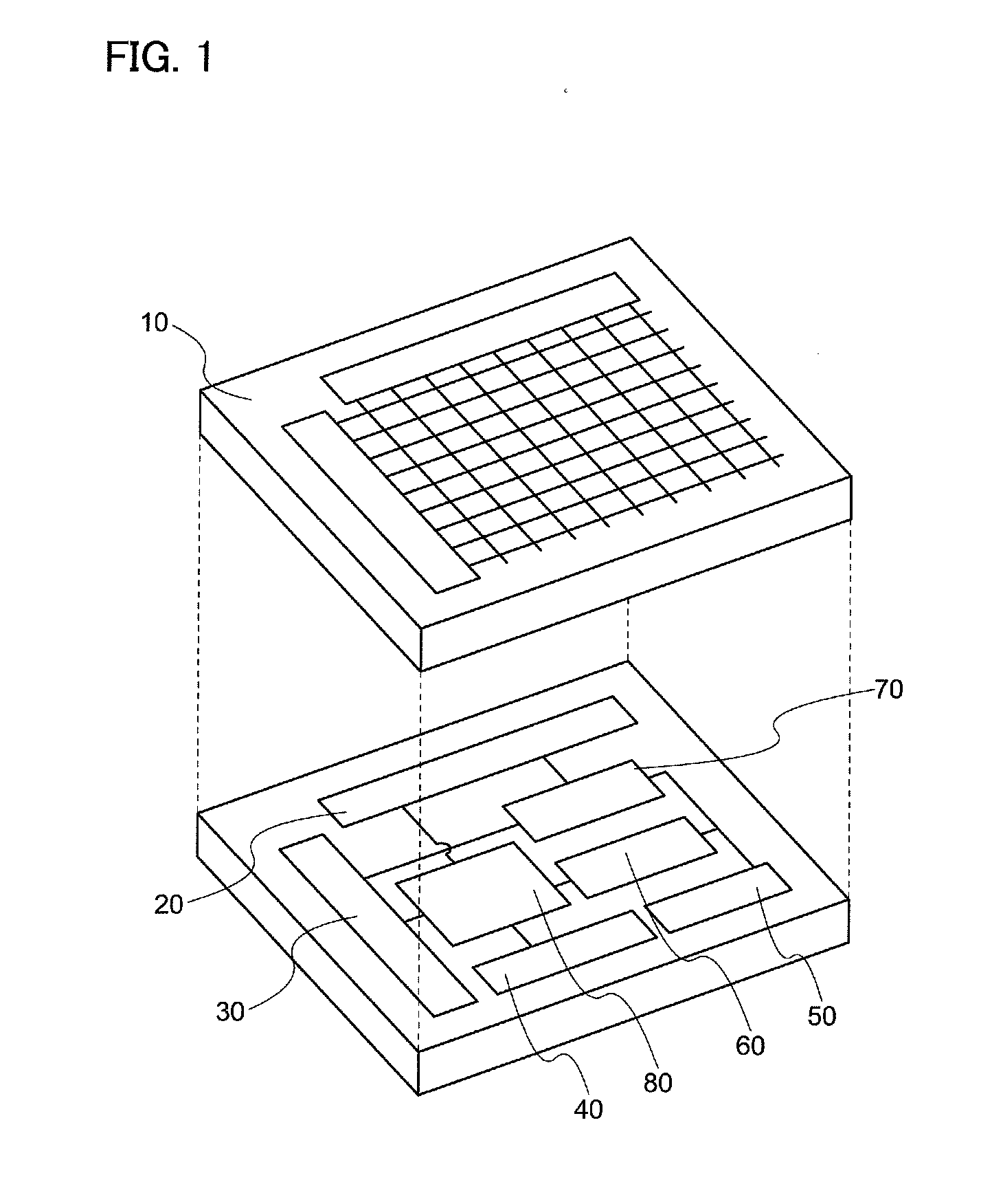
[0048]FIG. 1 is a schematic view illustrating an example of a structure of a semiconductor device. A semiconductor device according to one embodiment of the disclosed invention is, typically, a semiconductor device with a layered structure which includes a memory circuit in an upper portion and a logic circuit (also referred to as an arithmetic circuit) and a driver circuit which need high speed operation in a lower portion.

[0049]A semiconductor device illustrated in FIG. 1 is a semiconductor device (a memory device) including a memory cell array 10 in an upper portion, and a...

embodiment 2

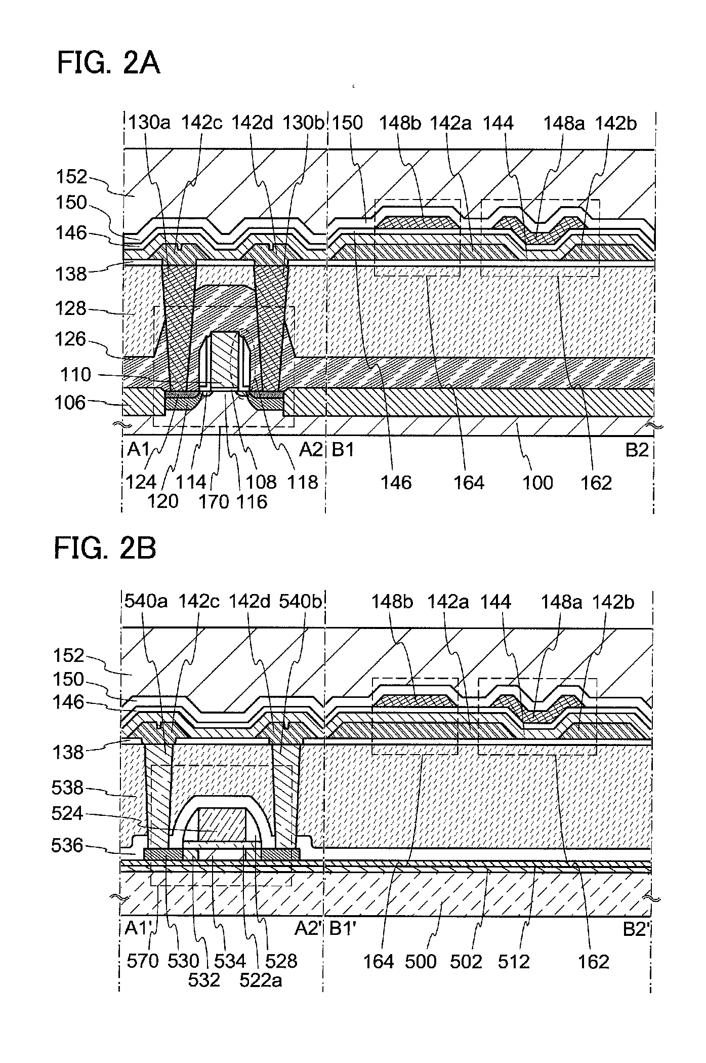
[0105]In this embodiment, a manufacturing method of a semiconductor device using an oxide semiconductor, specifically, a manufacturing method of the transistor 162 in an upper portion in FIGS. 2A and 2B is described with reference to FIGS. 6A to 6E. Note that since FIGS. 6A to 6E are cross-sectional views mainly illustrating the manufacturing steps and the like of the transistor 162, detailed description of the transistor 170 and the like below the transistor 162 is omitted.

[0106]First, the insulating layer 138 is formed over the interlayer insulating layer 128. After that, a conductive layer is formed over the insulating layer 138 and is selectively etched, so that the source or drain electrode 142a and the source or drain electrode 142b are formed (see FIG. 6A).

[0107]The insulating layer 138 functions as a base and can be formed by a PVD method, a CVD method, or the like. The insulating layer 138 can be formed using a material containing an inorganic insulating material such as si...

embodiment 3

[0144]In this embodiment, a manufacturing method of a transistor using an oxide semiconductor (especially, an oxide semiconductor having an amorphous structure) will be described with reference to FIGS. 7A to 7E. The transistor can be used instead of the transistor 162 or the like in any of the above embodiments. A structure of the transistor according to this embodiment and the structure of the transistor according to any of the above embodiments are partly common to each other. Therefore, a difference is mainly described below. A top-gate transistor is described below as an example; however, a structure of the transistor is not limited to a top-gate structure.

[0145]First, an insulating layer 202 is formed over an object 200. After that, an oxide semiconductor layer 206 is formed over the insulating layer 202 (see FIG. 7A).

[0146]The object 200 is, for example, the interlayer insulating layer 128 in any of the above embodiments. Arithmetic mean deviation (Ra) of a surface of the obj...


PUM


Abstract

An object of one embodiment of the present invention is to provide a semiconductor device with a novel structure in which stored data can be stored even when power is not supplied in a data storing time and there is no limitation on the number of times of writing. The semiconductor device includes a first transistor which includes a first channel formation region using a semiconductor material other than an oxide semiconductor, a second transistor which includes a second channel formation region using an oxide semiconductor material, and a capacitor. One of a second source electrode and a second drain electrode of the second transistor is electrically connected to one electrode of the capacitor.

Description

TECHNICAL FIELD[0001]The disclosed invention relates to a semiconductor device using a semiconductor element and a manufacturing method of the semiconductor device.BACKGROUND ART[0002]Memory devices using semiconductor elements are broadly classified into two categories: a volatile memory device that loses stored data when power supply stops, and a non-volatile memory device that stores stored data even when power is not supplied.[0003]A typical example of a volatile memory device is a DRAM (dynamic random access memory). A DRAM stores data in such a manner that a transistor included in a memory element is selected and charge is stored in a capacitor.[0004]When data is read from a DRAM, charge in a capacitor is lost on the above-described principle; thus, another writing operation is necessary whenever data is read out. Moreover, a transistor included in a memory element has leakage current and charge flows into or out of a capacitor even when the transistor is not selected, so that...

Claims


Application Information

Patent Timeline
Patent Type & Authority Applications(United States)
IPC IPC(8): H01L27/108H01L29/12
CPCG11C13/0007G11C13/003G11C2213/79H01L27/105H01L28/40H01L27/11H01L27/11551H01L27/1156H01L27/1225H01L27/108H10B12/00H10B10/00H10B41/70H10B41/20H10B99/00H01L27/124H01L27/1255H01L29/24H01L29/7869H01L29/78696
Inventor YAMAZAKI, SHUNPEIKOYAMA, JUNKATO, KIYOSHI
Owner SEMICON ENERGY LAB CO LTD
Why Eureka
Try Eureka