Methods of fabricating semiconductor structures or devices using layers of semiconductor material having selected or controlled lattice parameters

a technology of semiconductor material and fabrication method, which is applied in the direction of semiconductor devices, basic electric elements, electrical equipment, etc., can solve the problems of increasing the defect density, imposing limitations on the device that can be fabricated, and undesirable lattice strain in the layer of semiconductor material

Active Publication Date: 2011-06-30
S O I TEC SILICON ON INSULATOR THECHNOLOGIES
View PDF46 Cites 46 Cited by
  • Summary
  • Abstract
  • Description
  • Claims
  • Application Information

AI Technical Summary

Benefits of technology

[0015]In some embodiments, the present invention includes methods of fabricating semiconductor structures or devices. The methods may include changing a temperature of a layer of semiconductor material from a first temperature to a second temperature, and causing a lattice parameter of the layer of semiconductor material to change from a first value to a second value as the temperature of the layer of semiconductor material is changed from the first temperature to the second temperature. The layer of semiconductor material may be bonded to another layer of material while the layer of semiconductor material is at the second temperature. After bonding the layer of semiconductor material to another layer of material, the temperature of the layer of semiconductor material may be returned to the first temperature, and the lattice parameter of the layer of semiconductor material may be prevented from returning to the first value thereof upon returning the temperature of the layer of semiconductor material to the first temperature.

Problems solved by technology

There are various semiconductor devices and processes in which such lattice strain imposes limitations on the devices that can be fabricated.
The presence of such lattice strain in a layer of semiconductor material may be undesirable for a number of reasons.
For example, the presence of lattice strain in a layer of semiconductor material may result in an increased density of defects (e.g., lattice dislocations) in the layer of semiconductor material, undesirable morphology at the surface of the layer of semiconductor material, and may even result in the formation of cracks in the layer of semiconductor material.
Furthermore, the presence of lattice strain in a layer of semiconductor material may facilitate the onset of undesirable separation of material phases within the layer of semiconductor material.
It is difficult to form an indium gallium nitride seed layer on the surface of an engineered substrate in such a manner that the indium gallium nitride seed layer has a lattice parameter that will match that of an indium gallium nitride device layer to be formed thereover.
As an engineered substrate is cooled from such elevated temperatures to room temperature, any mismatch in the coefficient of thermal expansion between adjacent layers of material in the substrate can result in lattice strain in one or both of the adjacent layers of material upon cooling of the substrate.

Method used


Image

  • Methods of fabricating semiconductor structures or devices using layers of semiconductor material having selected or controlled lattice parameters
  • Methods of fabricating semiconductor structures or devices using layers of semiconductor material having selected or controlled lattice parameters
  • Methods of fabricating semiconductor structures or devices using layers of semiconductor material having selected or controlled lattice parameters

Examples


Embodiment Construction

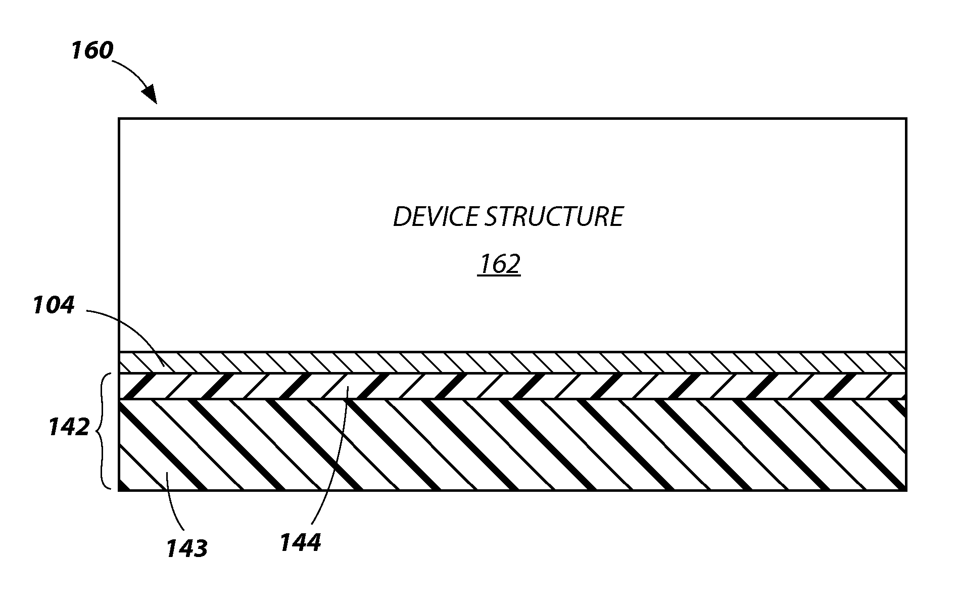
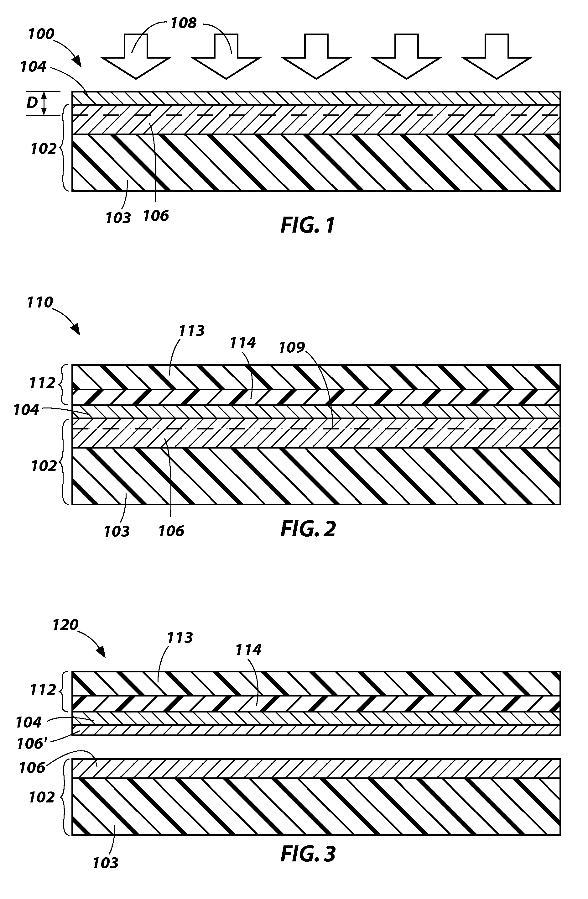
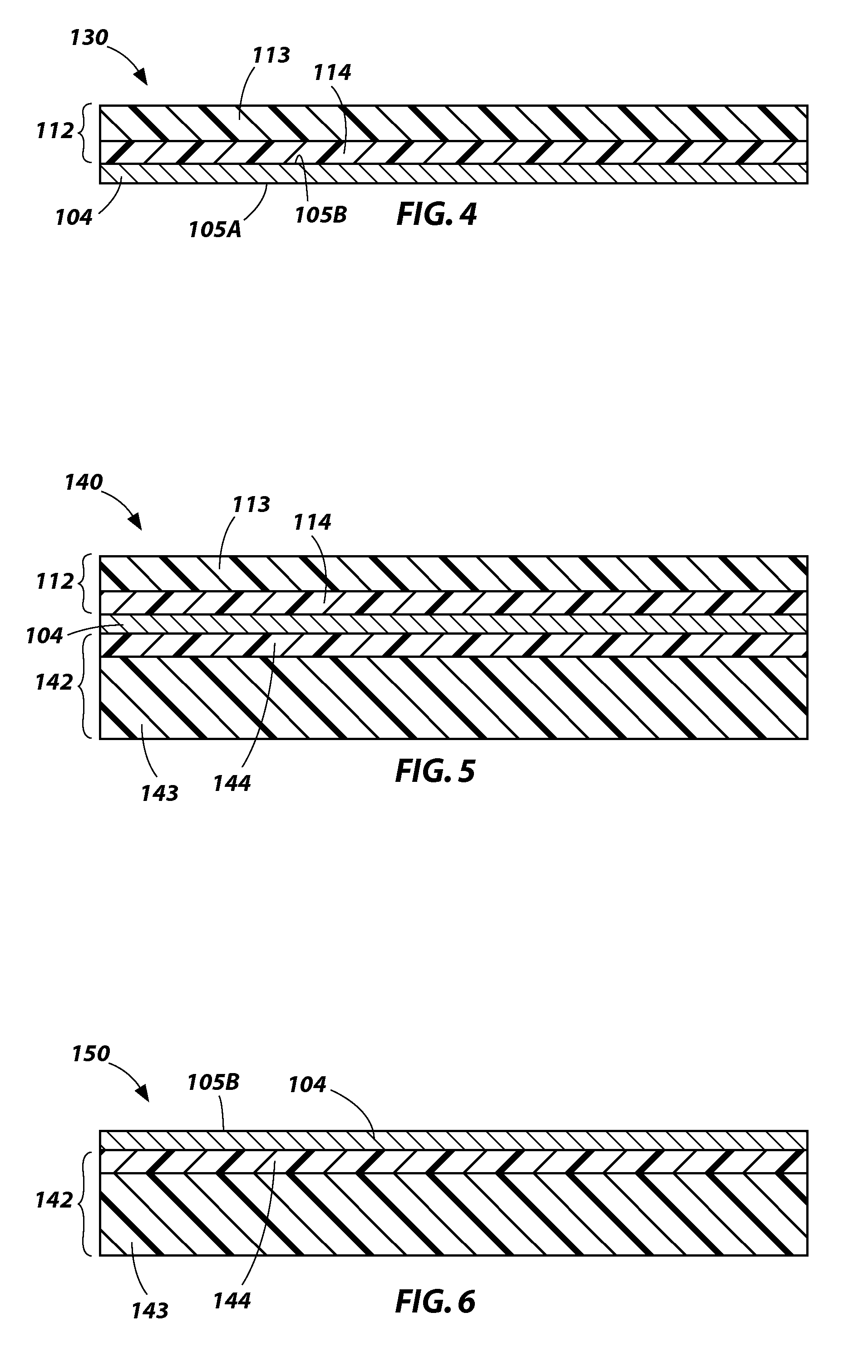
[0028]The illustrations presented herein are not meant to be actual views of any particular material, apparatus, system, or method, but are merely idealized representations which are employed to describe the present invention. Additionally, elements common between figures may retain the same numerical designation. As used herein, the term “III-V type semiconductor material” means and includes any material predominantly comprised of one or more elements from group IIIB of the periodic table (B, Al, Ga, In, and Ti) and one or more elements from group VB of the periodic table (N, P, As, Sb, and Bi).

[0029]As used herein, the term “II-VI type semiconductor material” means and includes any material predominantly comprised of one or more elements from group IIB of the periodic table (Zn, Cd, and Hg) and one or more elements from group VIB of the periodic table (O, S, Se, Te, and Po).

[0030]As used herein, the term “coefficient of thermal expansion,” when used with respect to a material or s...


PUM

PropertyMeasurementUnit
thicknessaaaaaaaaaa
thicknessaaaaaaaaaa
temperatureaaaaaaaaaa

Abstract

Methods of fabricating semiconductor devices or structures include bonding a layer of semiconductor material to another material at a temperature, and subsequently changing the temperature of the layer of semiconductor material. The another material may be selected to exhibit a coefficient of thermal expansion such that, as the temperature of the layer of semiconductor material is changed, a controlled and/or selected lattice parameter is imparted to or retained in the layer of semiconductor material. In some embodiments, the layer of semiconductor material may comprise a III-V type semiconductor material, such as, for example, indium gallium nitride. Novel intermediate structures are formed during such methods. Engineered substrates include a layer of semiconductor material having an average lattice parameter at room temperature proximate an average lattice parameter of the layer of semiconductor material previously attained at an elevated temperature.

Description

PRIORITY CLAIM[0001]This application claims the benefit of the filing date of U.S. Provisional patent application Ser. No. 61 / 092,373, filed Aug. 27, 2008, for “Methods of Fabricating Semiconductor Structures or Devices Using Layers of Semiconductor Material Having Selected or Controlled Lattice Parameters.”TECHNICAL FIELD[0002]The present invention generally relates to the fabrication of semiconductor structures or devices using engineered substrates, to intermediate structures formed during the fabrication of semiconductor structures or devices, and to engineered substrates for use in the fabrication of semiconductor structures or devices.BACKGROUND[0003]Substrates that include one or more layers of semiconductor material are used to form a wide variety of semiconductor structures and devices including, for example, integrated circuit (IC) devices (e.g., logic processors and memory devices), radiation emitting devices (e.g., light emitting diodes (LEDs), resonant cavity light emit...

Claims


Application Information

Patent Timeline
Patent Type & Authority Applications(United States)
IPC IPC(8): H01L29/20H01L21/324
CPCH01L21/187H01L29/2003H01L33/0079H01L21/76254H01L33/0093H01L33/00
Inventor ARENA, CHANTAL
Owner S O I TEC SILICON ON INSULATOR THECHNOLOGIES
Why Eureka
Try Eureka