Liquid crystal display device and electronic device

Inactive Publication Date: 2011-06-30
SEMICON ENERGY LAB CO LTD
View PDF68 Cites 67 Cited by
  • Summary
  • Abstract
  • Description
  • Claims
  • Application Information

AI Technical Summary

Benefits of technology

[0010]An object of one embodiment of the present invention is to provide a liquid crystal display device of which

Problems solved by technology

Since a backlight is used in a transmissive liquid crystal display device, it is difficult to recognize display in an environment where external light is strong such as outdo

Method used


Image

  • Liquid crystal display device and electronic device
  • Liquid crystal display device and electronic device
  • Liquid crystal display device and electronic device

Examples


embodiment 1

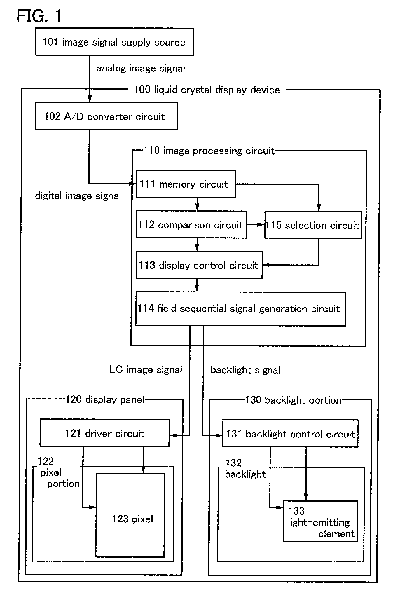
[0044]In this embodiment, a liquid crystal display device including a still-image display mode and a moving-image display mode will be described with reference to FIG. 1.

[0045]In this specification, a still-image display mode refers to an operation performed when the liquid crystal display device judges an image signal input as a still image, and a moving-image display mode refers to an operation performed when the liquid crystal display device judges an image signal input as a moving image.

[0046]A liquid crystal display device 100 according to this embodiment includes an A / D converter circuit 102, an image processing circuit 110, a display panel 120, and a backlight portion 130.

[0047]The image processing circuit 110 includes a memory circuit 111, a comparison circuit 112, a display control circuit 113, a field sequential signal generation circuit 114 and a selection circuit 115.

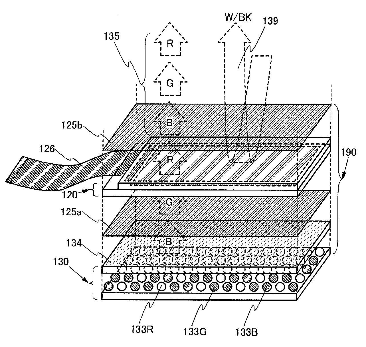
[0048]The display panel 120 includes a driver circuit 121 and a pixel portion 122. In the pixel portion 1...

embodiment 2

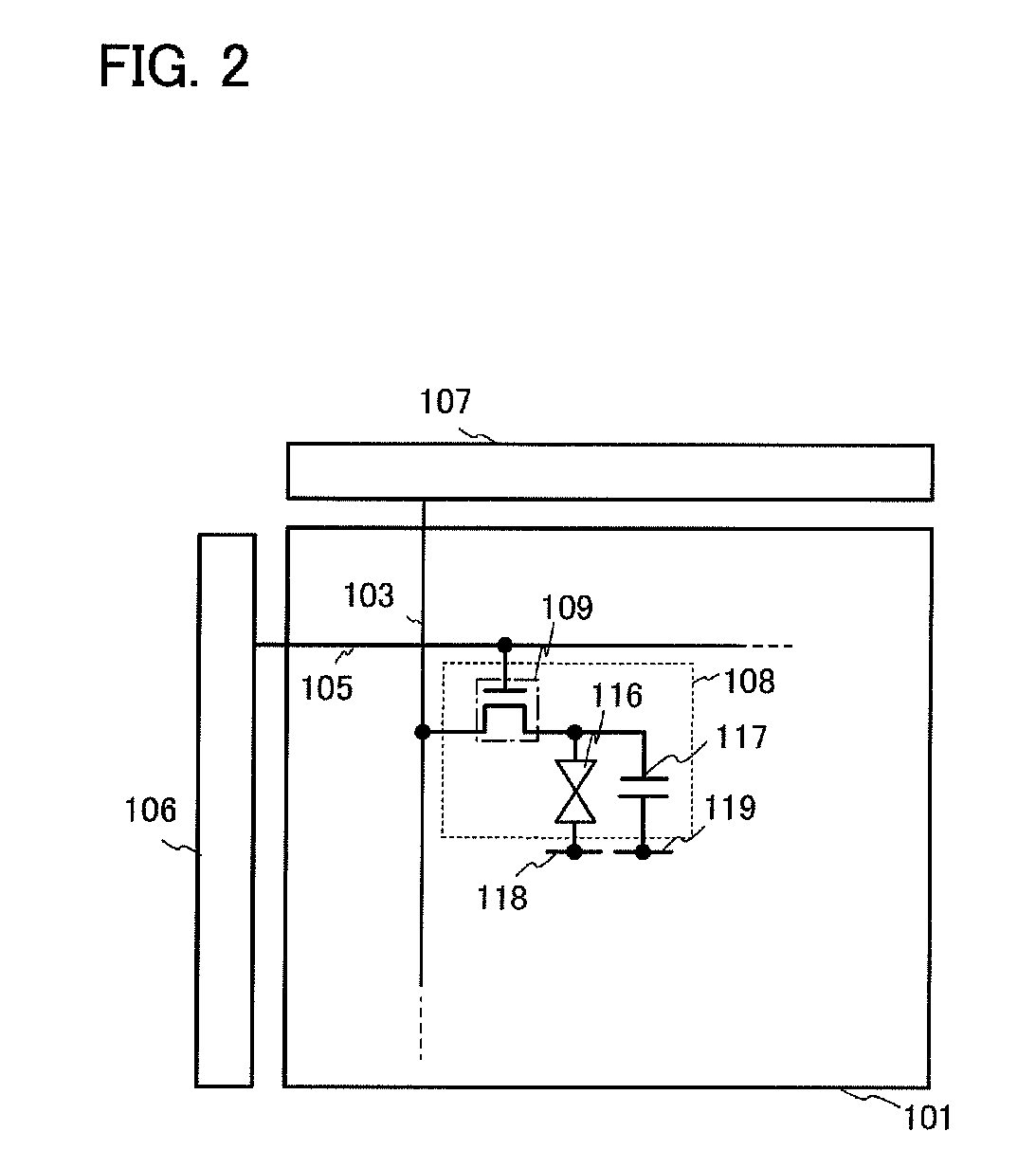
[0090]In this embodiment, a driving method of a liquid crystal display device will be described using a pixel connection diagram, a timing chart, and the like. First, FIG. 2 is a schematic view of a display panel of a liquid crystal display device. In FIG. 2, the display panel includes a pixel portion 101, a scan line 105 (also referred to as a gate line), a signal line 103 (also referred to as a data line), a pixel 108, a common electrode 118, a capacitor line 119, a scan line driver circuit 106, and a signal line driver circuit 107.

[0091]The pixel 108 includes a pixel transistor 109, a liquid crystal element 116, and a capacitor 117. A gate of the pixel transistor 109 is connected to the scan line 105, a first terminal serving as one of a source and a drain of the pixel transistor 109 is connected to the signal line 103, and a second terminal serving as the other of the source and the drain of the pixel transistor 109 is connected to one electrode of the liquid crystal element 116...

embodiment 3

[0109]In this embodiment, a structure of a driving method of the liquid crystal display device which is different from that of the driving method described in Embodiment 2 will be described using a timing chart and the like. First, a timing chart illustrated in FIG. 4A is used to describe a driving method of the backlight in the moving-image display period 301 described in Embodiment 2.

[0110]The timing chart in FIG. 4A is different from that in FIG. 3B in that a non-lighting period of the backlight (BL in FIG. 4A) is provided after the lighting of the backlight following the writing of an image signal. Flicker of color or the like can be reduced and visibility can be improved by providing a period during which the backlight is turned off before writing the next image signal.

[0111]FIG. 4B illustrates a structure different from that in FIG. 4A. The timing chart in FIG. 4B is different from that in FIG. 4A in that a light-emitting period of blue (B) is provided instead of the non-light...


PUM


Abstract

An object is to provide a liquid crystal display device in which image display can be recognized even in an environment where light is dim around the liquid crystal display device. Another object is to provide a liquid crystal display device capable of image display in both modes of a reflective mode in which external light is used as a light source and a transmissive mode in which a backlight is used. One pixel is provided with a pixel electrode having both of a region where light incident through a liquid crystal layer is reflected and a region having a light-transmitting property, so that image display can be performed in both modes of a reflective mode in which external light is used as a light source and a transmissive mode in which a backlight is used.

Description

TECHNICAL FIELD[0001]The present invention relates to a liquid crystal display device including a transistor such as a thin film transistor (hereinafter, referred to as a TFT) and a manufacturing method thereof. The present invention further relates to an electronic device on which the liquid crystal display device is mounted as a component.BACKGROUND ART[0002]In a liquid crystal display device, an active matrix liquid crystal display device in which pixel electrodes are arranged in matrix and transistors are used as switching elements connected to respective pixel electrodes in order to obtain a high-quality image, has attracted attention.[0003]An active matrix liquid crystal display device including transistors, in which metal oxide is used as a channel formation region, as switching elements connected to respective pixel electrodes is already known (Patent Documents 1 and 2).[0004]It is known that active matrix liquid crystal display devices are roughly divided into two kinds: a ...

Claims


Application Information

Patent Timeline
IPC IPC(8): G09G3/36G09G5/10
CPCG02F1/133555G09G3/3406G09G3/3413G09G3/3648G09G2300/0456G09G2310/0235G09G2360/144G09G2320/0261G09G2320/103G09G2330/021G09G2340/0435G09G2340/06G09G2320/0247
Inventor YAMAZAKI, SHUNPEIKOYAMA, JUNHIRAKATA, YOSHIHARU
Owner SEMICON ENERGY LAB CO LTD
Why Eureka
Try Eureka