2-phase gain calibration and scaling scheme for switched capacitor sigma-delta modulator using a chopper voltage reference

a sigma-delta modulator and switched capacitor technology, applied in the field of analog-to-digital converters, can solve problems such as large errors, modulators giving erroneous results, and modulators becoming unstabl

Active Publication Date: 2011-07-07
MICROCHIP TECH INC
View PDF15 Cites 35 Cited by
  • Summary
  • Abstract
  • Description
  • Claims
  • Application Information

AI Technical Summary

Benefits of technology

[0012]According to a further embodiment of the method, a switching sequence may be selected from all possible switching sequences depending on a current output value of the DAC and a current offset state of the chopper voltage reference. According to a further embodiment of the method, for a first sub-set of DAC output values a switching sequence can be selected depending only on a current output value of the DAC and for a remaining sub-set of DAC output values, a switching sequence can be selected depending on a current output value of the DAC and a current offset state of the chopper voltage reference. According to a further embodiment of the method, in a five-level DAC, the first sub-set may include even output values and the remaining sub-set may include odd output values. According to a further embodiment of the method, during a first sample, a first capacitor pair can be used for sampling an input signal in a charge phase and transfer phase and the second capacitor pair for sampling a reference signal in a charge phase and transfer phase in parallel with said input signal; During a following sample, using the second capacitor pair for sampling an input signal in a charge phase and transfer phase and the first capacitor pair for sampling a reference signal in a charge phase and transfer phase in parallel with said input signal. According to a further embodiment of the method, the method may further comprise coupling each pair of capacitors with one of: a positive input signal line, a negative input signal line, a positive reference signal line, a negative reference signal line, and a common ground potential. According to a further embodiment of the method, for a charge transfer, during a charge phase, the input signal or reference signal can be connected on one side of a pair of capacitors which is otherwise coupled with a common ground potential, and during a transfer phase, connecting the one side of the pair of capacitors with each other or coupling the one side with an inverted input or reference signal. According to a further embodiment of the method, for a zero charge transfer the method may comprise, during a charge phase, connecting one side of a pair of capacitors with each other and connecting the common ground potential on the other side of said pair of capacitors, and during a transfer phase, connecting the one side of the pair of capacitors again with each other. According to a further embodiment of the method, more than two capacitor pairs can be provided, the method may comprise the steps of: During a first sample, selecting a first subset of capacitor pairs from a plurality of capacitor pairs for sampling an input signal in a charge phase and transfer phase and selecting a second subset from the remaining capacitor pairs of said plurality of capacitor pair for sampling a reference signal in a charge phase and transfer phase in parallel with said input signal; Repeating said steps for following samplings, wherein another first and second subset of capacitor pairs is selected that is different from a previously selected first and second subset. According to a further embodiment of the method, the first subset may comprise a plurality of capacitor pairs and the second subset may comprise the remaining capacitor pairs from said more than two capacitor pairs. According to a further embodiment of the method, a gain can be achieved by a ratio of the number of capacitor pairs assigned to the input signal and the number of pairs assigned to the reference signal. According to a further embodiment of the method, the chopper voltage reference can be clocked by a clock controlling said two phases.

Problems solved by technology

Outside of this stable input range the error becomes very large and the modulator gives erroneous results.
Above this range the modulator becomes unstable.
However, if these voltages are sampled on different capacitors, the mismatch error of the capacitors will produce a gain error on the output result of the sigma-delta ADC.
The other drawback of this technique is that you cannot sample two voltages on one capacitors, so the sampling of the input signal and DAC voltage have to be done one after the other resulting in a 4-phase system: 2 phases to sample and transfer charges coming from the input signals, and then 2 phases to sample and transfer charges coming from DAC voltage.
This 4-phase system is less efficient because the sampling is done in series and consumes more time than if the DAC voltage and input voltage sampling were done in parallel.
However requiring four steps (phases) per sample limits the sample rate of the sigma-delta modulator, and / or requires much faster operating speed (faster clocking and higher frequency operation components with a subsequence increase in power usage) of the sigma-delta modulator to complete a signal conversion in a desired time frame.

Method used


Image

  • 2-phase gain calibration and scaling scheme for switched capacitor sigma-delta modulator using a chopper voltage reference
  • 2-phase gain calibration and scaling scheme for switched capacitor sigma-delta modulator using a chopper voltage reference
  • 2-phase gain calibration and scaling scheme for switched capacitor sigma-delta modulator using a chopper voltage reference

Examples


Embodiment Construction

sible states for each stage (in this representation the number of input stages is limited to 5);

[0021]FIG. 7 shows an example of a rotation algorithm to perform the 2-phase gain scaling and gain error cancellation which is not depending on the DAC input states;

[0022]FIGS. 8a and b show another example of a rotation algorithm to perform the 2-phase gain scaling and gain error cancellation, but which is depending on the DAC input states;

[0023]FIG. 9 shows the state diagram for the rotation algorithm that is depending on the DAC states (DAC input dependent algorithm) and that performs gain scaling and gain error cancellation;

[0024]FIG. 10 shows a block diagram of a chopper voltage reference; and

[0025]FIG. 11 shows an example of yet another rotation algorithm when a chopped voltage reference is used.

DETAILED DESCRIPTION

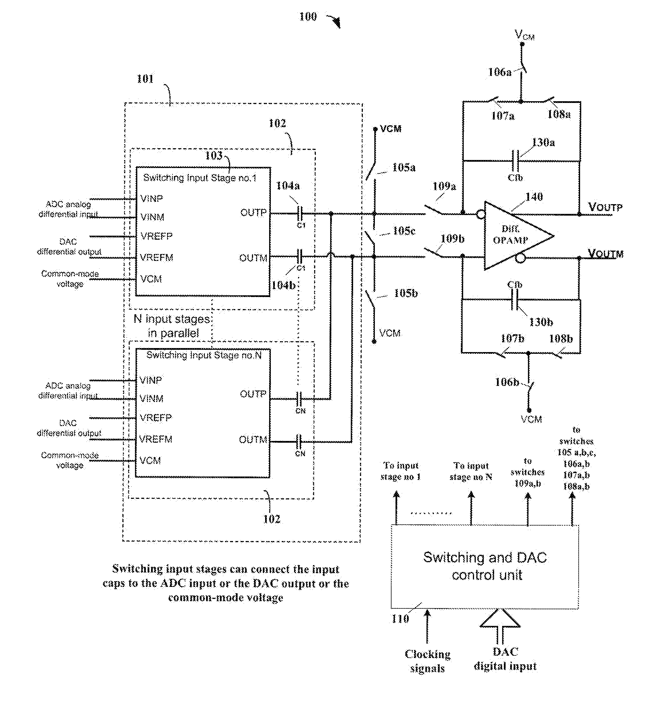
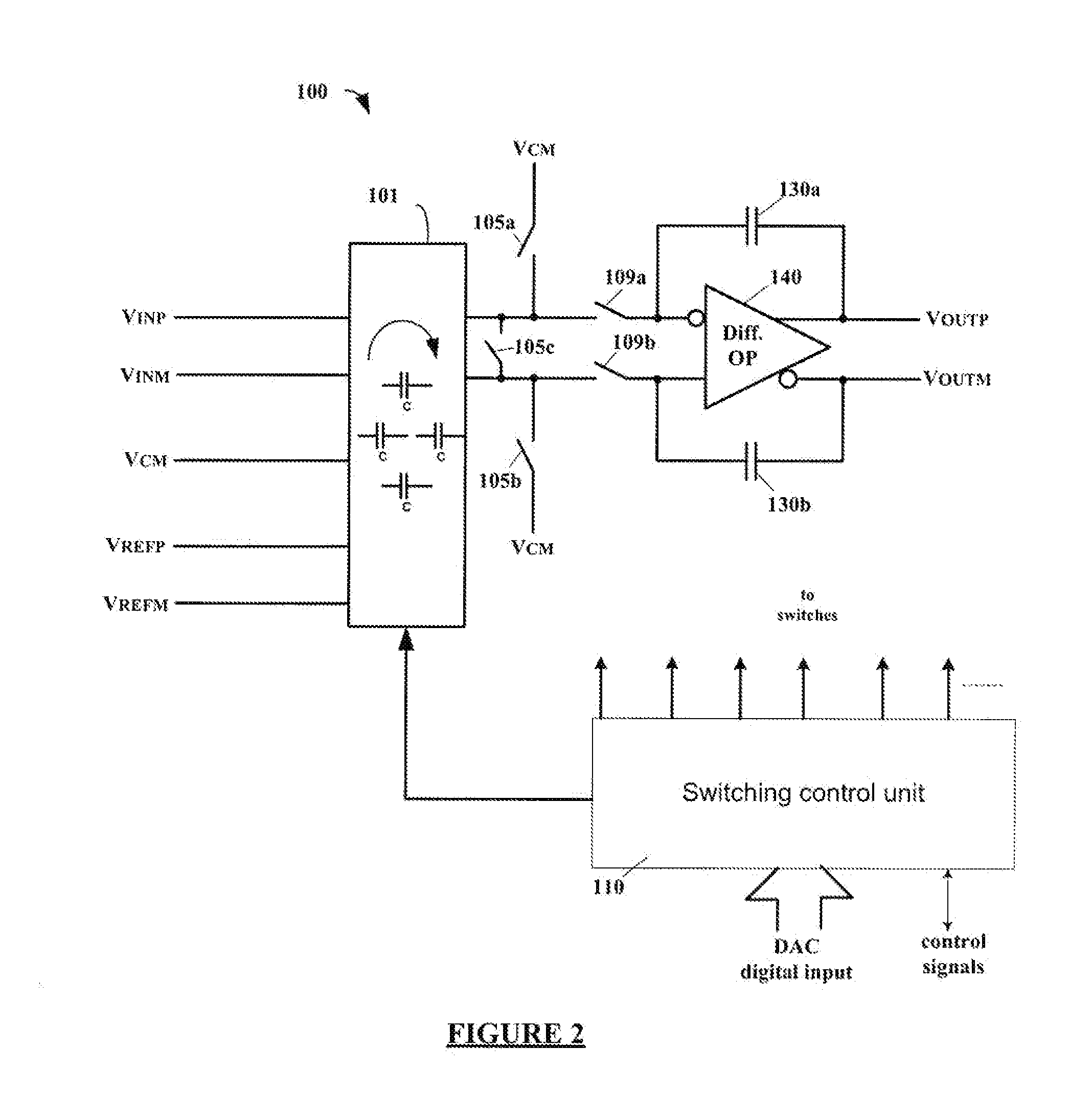
[0026]According to various embodiments, a sigma-delta modulator that can use only two phases instead of four per each sample with less power consumption (due to less stri...


PUM


Abstract

A sigma-delta modulator has a chopper voltage reference providing a reference signal having a clock dependent offset voltage, a single-bit or a multi-bit digital-to-analog converter (DAC); a plurality of capacitor pairs; a plurality of switches to couple any capacitor pair to an input or reference signal; and a control unit controlling sampling through said switches to perform a charge transfer in two phases wherein any capacitor pair can be selected to be assigned to the input or reference signal, wherein after a plurality of charge transfers a gain error cancellation is performed by rotating the capacitor pairs cyclically, and wherein a DAC output value and a reference offset state define switching sequences wherein each switching sequence independently rotates said capacitor pairs and wherein at least one switching sequence is selected depending on a current DAC output value and a current reference offset state.

Description

CROSS-REFERENCE TO RELATED APPLICATIONS[0001]This application is a continuation-in-part of U.S. patent application Ser. No. 12 / 832,599 filed on Jul. 8, 2010, which claims the benefit of U.S. Provisional Application No. 61 / 226,049 filed on Jul. 16, 2009, the contents of which are hereby incorporated by reference in their entirety.TECHNICAL FIELD[0002]The present disclosure relates to analog-to-digital converters, in particular to sigma-delta modulators and, more particularly, to a way of reducing the gain error due to influence of mismatched capacitors in sigma-delta modulators, with no penalty on the conversion time.BACKGROUND[0003]Analog-to-digital converters (ADC) are in widespread use today in electronics for consumers, industrial applications, etc. Typically, analog-to-digital converters include circuitry for receiving an analog input signal and outputting a digital value proportional to the analog input signal. This digital output value is typically in the form of either a para...

Claims


Application Information

Patent Timeline
Patent Type & Authority Applications(United States)
IPC IPC(8): H03M3/02
CPCH03M1/0663H03M1/0665H03M3/464H03M3/456H03M3/422
Inventor QUIQUEMPOIX, VINCENTJOHNER, YANNBELLINI, GABRIELE
Owner MICROCHIP TECH INC
Why Eureka
Try Eureka