Increased receive sensitivity radio frequency front end integrated circuits

a front-end integrated circuit and receive-sensitive technology, applied in the direction of transmission, electrical equipment, etc., can solve the problems of increasing the transformation coefficient from the antenna to the low-noise amplifier input, the receive chain of the front-end circuit tends to exhibit increased noise figures, and the conventional wireless communication transceiver typically does not generate sufficient power or have the sensitivity necessary for reliable communication, etc., to achieve low noise, reduce the effect of resistance and high transistor impedan

Active Publication Date: 2011-07-07
SKYWORKS SOLUTIONS INC
View PDF14 Cites 19 Cited by
  • Summary
  • Abstract
  • Description
  • Claims
  • Application Information

AI Technical Summary

Benefits of technology

[0011]In accordance with various embodiments of the present disclosure, a front end circuit for coupling an antenna to a radio frequency (RF) transceiver is contemplated. The RF transceiver has a defined operating frequency band, as well as a signal input, a signal output, a receive enable line activated during a receive mode and transmit enable line activated during a transmit mode. The front end circuit may include an antenna port connectible to the antenna. Additionally, the front end circuit may include a power amplifier that is coupled to the signal output of the RF transceiver. The power amplifier may include a transmit control circuit coupled to the transmit enable line of the RF transceiver. Furthermore, the front end circuit may include a low noise amplifier that is coupled to the signal input of the RF transceiver. The low noise amplifier may likewise include a receive control circuit coupled to the receive enable line of the RF transceiver. There may also be a switching network that is connected to the antenna port, the power amplifier, and the low noise amplifier. The switching network may include at least one resonant circuit and a control circuit coupled to the receive enable line of the transceiver. This resonant circuit may define a parallel resonance with a first resonant resistance in the operating frequency band upon activation in the receive mode. The resonant circuit may also define a substantially high transistor impedance upon deactivation in the transmit mode.
[0012]The present disclosure contemplates the independent configuration of the transmit chain based upon its linearity requirements, as well as the independent configuration of the receive chain based upon its noise figure requirements. In particular, the resistive part of impedance of the power amplifier output matching is not tied to the resistive part of the low noise amplifier base-emitter impedance. The power amplifier output matching circuit is understood to require smaller resistances due to the increased power levels, and the low noise amplifier input matching circuit can have a higher input impedance. Accordingly, the overall loss of the low noise amplifier input matching circuit is minimized with a resulting improvement in the overall noise figure. The present invention will be best understood by reference to the following detailed description when read in conjunction with the accompanying drawings.

Problems solved by technology

Conventional wireless communication transceivers typically do not generate sufficient power or have sufficient sensitivity necessary for reliable communications.
With communication systems that require substantially higher transmit power in relation to received signals such as WiMAX (IEEE 802.16), however, the receive chain of the front end circuit tended to exhibit increase noise figures.
This is understood to result in a higher transformation coefficient from the antenna to the low noise amplifier input, and corresponding resistive losses that are associated with the matching network.

Method used


Image

  • Increased receive sensitivity radio frequency front end integrated circuits
  • Increased receive sensitivity radio frequency front end integrated circuits
  • Increased receive sensitivity radio frequency front end integrated circuits

Examples


first embodiment

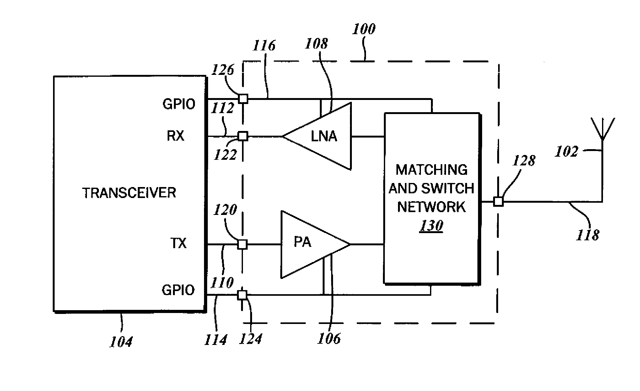
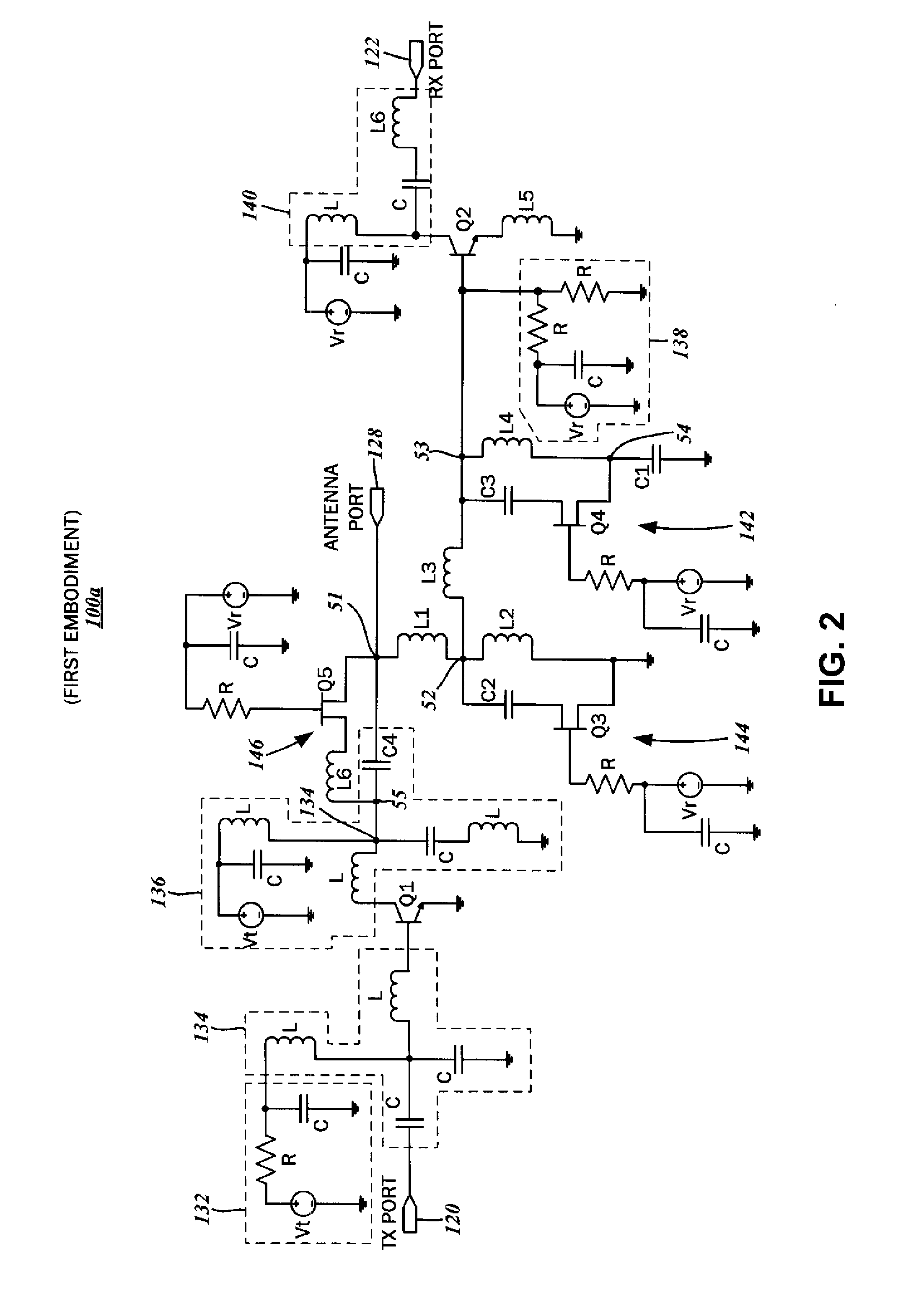
[0045]The circuit diagram of FIG. 2 illustrates the front end circuit 100a, including the transmit port 120, the receive port 122, and the antenna port 128. The transistor Q1 generally corresponds to the power amplifier 106, and is in a common-emitter configuration with a single amplification stage. The transistor Q2 generally corresponds to the low noise amplifier 108, and is also in a common-emitter configuration with a single amplification stage. It is understood that multi-stage amplifiers may be utilized for higher gain applications, and those having ordinary skill in the art will recognize the appropriate modifications to the basic configuration presented herein for such multi-stage amplifiers. In some embodiments, it is contemplated that the various transistors of the front end circuit 100, including transistors Q1 and Q2, have a bipolar junction structure. In other embodiments, the transistors may have a field-effect structure (MOSFET, MESFET, etc.) While the present disclos...

second embodiment

[0067]the front end circuit 100b contemplates the matching and switch network 130 including the first resonant circuit 142 with the corresponding RF switching transistor Q4, and the second resonant circuit 144 with the corresponding RF switching transistor Q3. Again, although a field effect transistor is utilized, any other type of transistor may be substituted. The second resonant circuit 144 is connected to the inductor L1 at the second node 52.

[0068]The transistor Q1, which corresponds to the power amplifier 106, is activated in the transmit mode. However, the transistor Q2, which corresponds to the low noise amplifier 108, is deactivated. Additionally, the RF switching transistors Q3 and Q4 are deactivated. Thus, the low noise amplifier 108 and the RF switching transistors Q3 and Q4 are selectively activated in a substantially exclusive relation to the power amplifier 106. In the deactivated state, it is understood that the transistors Q3 and Q4 have a substantially high impedan...

third embodiment

[0080]the front end circuit 100c contemplates the matching and switch network 130 including the first resonant circuit 142 with the corresponding RF switching transistor Q4, the second resonant circuit 144 with the corresponding RF switching transistor Q3, and the third resonant circuit 146 with the corresponding RF switching transistor Q5. Again, although a field effect transistor is utilized, any other type of transistor may be substituted. The second resonant circuit 144 is connected to the inductor L1 at the second node 52, while the third resonant circuit 146 is connected to the second node 52 and the third node 53 that is connected to the first resonant circuit 142 and the base of the low noise amplifier transistor Q2.

[0081]The transistor Q1, which corresponds to the power amplifier 106, and the RF switching transistor Q5 are activated in the transmit mode. Concurrently, the transistor Q2, which corresponds to the low noise amplifier 108, is deactivated. The RF switching trans...


PUM


Abstract

A front end circuit for coupling an antenna to a radio frequency (RF) transceiver is disclosed. An antenna port connectible to the antenna is provided, as well as a power amplifier coupled to a signal output of the RF transceiver and a low noise amplifier coupled to the signal input of the RF transceiver. The front end circuit includes a switching network that is connected to the antenna port, the power amplifier, and the low noise amplifier. Additionally, there is at least one resonant circuit and a control circuit coupled to a receive enable line of the transceiver. This resonant circuit defines a parallel resonance with a first resonant resistance in the operating frequency band upon activation in the receive mode. The resonant circuit also defines a substantially high transistor impedance upon deactivation in the transmit mode.

Description

CROSS-REFERENCE TO RELATED APPLICATIONS[0001]This application relates to and claims the benefit of U.S. Provisional Application No. 61 / 292,676, filed Jan. 6, 2010 and entitled TRANSMIT-RECEIVE RF FRONT-END IC CIRCUITS WITH INCREASED RX SENSITIVITY, which is wholly incorporated by reference herein.STATEMENT RE: FEDERALLY SPONSORED RESEARCH / DEVELOPMENT[0002]Not ApplicableBACKGROUND[0003]1. Technical Field[0004]The present invention relates generally to radio frequency (RF) signal circuitry, and more particularly, to transmit-receive RF front end integrated circuits with increased receive sensitivity.[0005]2. Related Art[0006]Wireless communications systems find application in numerous contexts involving information transfer over long and short distances alike, and there exists a wide range of modalities suited to meet the particular needs of each. These systems include cellular telephones and two-way radios for distant voice communications, as well as shorter-range data networks for c...

Claims


Application Information

Patent Timeline
Patent Type & Authority Applications(United States)
IPC IPC(8): H04B1/44
CPCH04B1/48H04B1/18
Inventor GORBACHOV, OLEKSANDR
Owner SKYWORKS SOLUTIONS INC
Why Eureka
Try Eureka