Real time monitoring of indium bump reflow and oxide removal enabling optimization of indium bump morphology

a technology of indium bumps and real-time monitoring, which is applied in the field of semiconductor devices, can solve the problems of inability to obtain a reliable, high-density bump pattern high-quality process, and the tendency of indium bumps to oxidize,

Inactive Publication Date: 2011-07-14
CALIFORNIA INST OF TECH
View PDF8 Cites 8 Cited by
  • Summary
  • Abstract
  • Description
  • Claims
  • Application Information

AI Technical Summary

Benefits of technology

[0014]The materials may include one or more metal electrical contact pads that are lithographically patterned on a device, and the solder bumps may be at least partially positioned on the surfaces of the one or more metal electrical contact pads. The controlling may correct for imperfect alignment of the solder bumps relative to the one or more metal electrical contact pads.
[0015]The controlling may achieve the solder bumps that are contained on the one or more metal electrical contact pads.

Problems solved by technology

While indium bump technology has been a part of the electronic interconnect process field for many years, and has been extensively employed in the infrared imager industry, obtaining a reliable, high yield process for high density patterns of bumps can be quite difficult.
One problem is the tendency of the indium bumps to oxidize during exposure to air.
Occasionally, errors in the patterning process lead to misaligned or misshapen bumps.
This is undesirable as it may affect the reliability of the electrical connection.

Method used


Image

  • Real time monitoring of indium bump reflow and oxide removal enabling optimization of indium bump morphology
  • Real time monitoring of indium bump reflow and oxide removal enabling optimization of indium bump morphology
  • Real time monitoring of indium bump reflow and oxide removal enabling optimization of indium bump morphology

Examples


Embodiment Construction

[0047]In the following description of the preferred embodiment, reference is made to the accompanying drawings which form a part hereof, and in which is shown by way of illustration a specific embodiment in which the invention may be practiced. It is to be understood that other embodiments may be utilized and structural changes may be made without departing from the scope of the present invention.

[0048]Overview

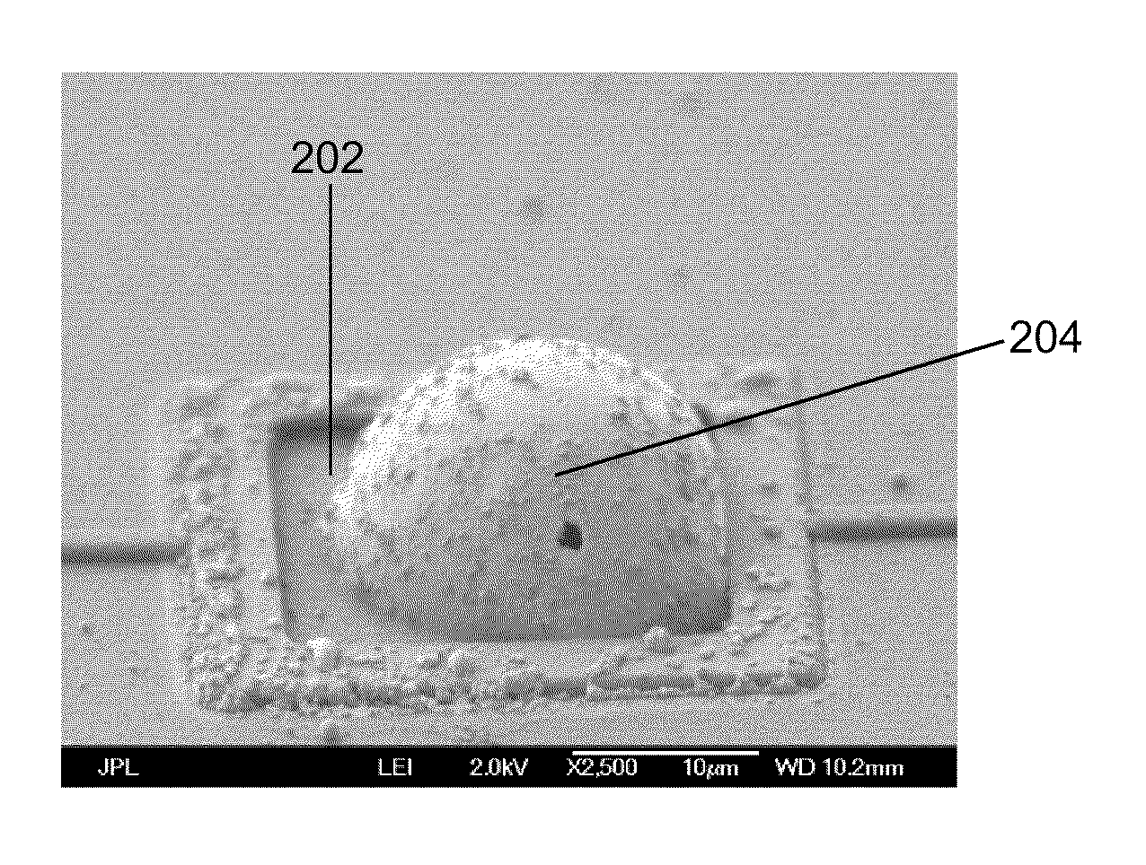
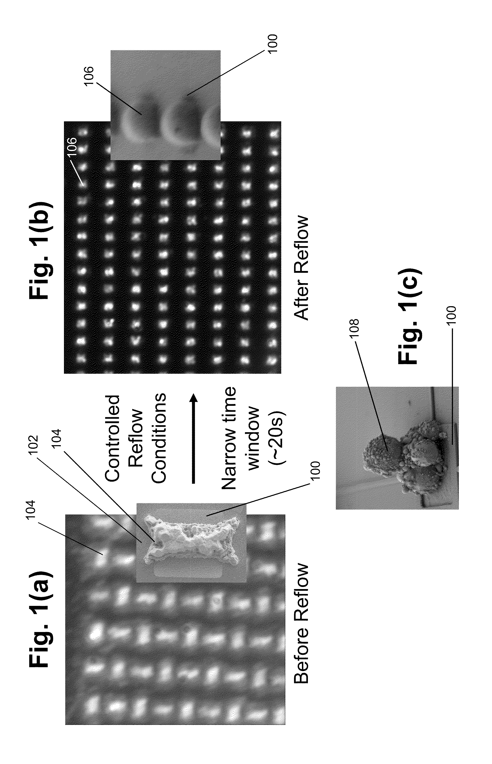
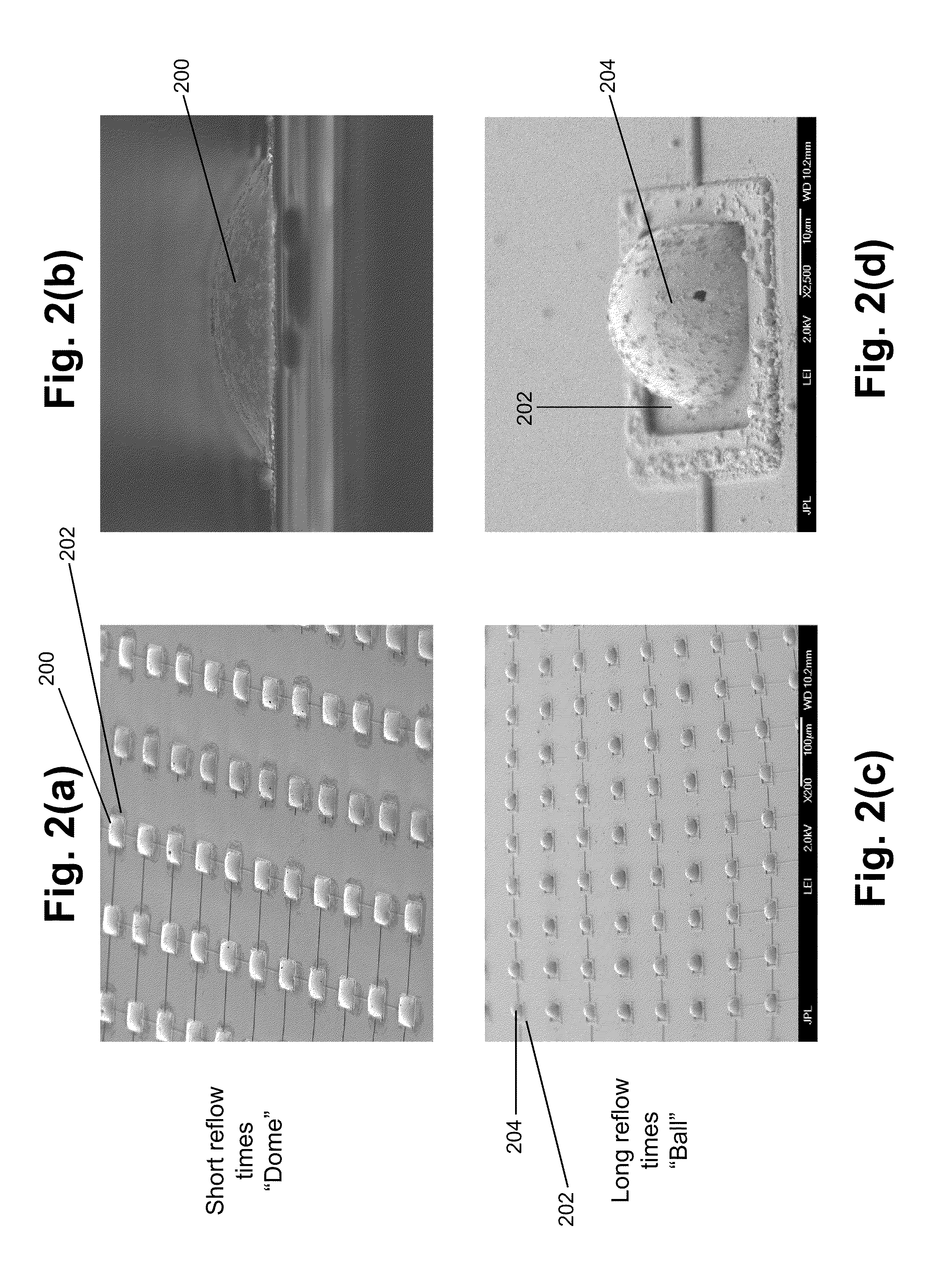
[0049]One or more embodiments of the present invention include both a process for removing indium oxide from indium bumps used in flip chip hybridization (bump bonding), a process for reflowing these indium bumps into a highly wetted configuration (dome shape) versus less desirable unwetted shapes (rectangles or spheres), and a way to monitor this transition in real time. This is the first known demonstration of the production of indium “domes” for hybridization. The reflow and indium oxide removal processes are attained by exposing detector and readout samples, with indium bu...


PUM

PropertyMeasurementUnit
heightaaaaaaaaaa
sizeaaaaaaaaaa
sizeaaaaaaaaaa

Abstract

A method, apparatus, system, and device provide the ability to form one or more solder bumps on one or more materials. The solder bumps are reflowed. During the reflowing, the solder bumps are monitored in real time. The reflow is controlled in real time, thereby controlling a morphology of each of the solder bumps. Further, the wetting of the solder bumps to a surface of the materials is controlled in real time.

Description

CROSS REFERENCE TO RELATED APPLICATIONS[0001]This application claims the benefit under 35 U.S.C. Section 119(e) of the following co-pending and commonly assigned U.S. Provisional Patent Application:[0002]U.S. Provisional Patent Application Ser. No. 61 / 294,754 filed on Jan. 13, 2010, by Todd J. Jones, Shouleh Nikzad, Thomas J. Cunningham, Edward R. Blazejewski, Matthew R. Dickie, Michael E. Hoenk and Harold Greer, entitled “REAL TIME MONITORING OF INDIUM BUMP RELFOW AND OXIDE REMOVAL ENABLING OPTIMIZATION OF INDIUM BUMP MORPHOLOGY” attorney's docket number 176.61-US-P1 (CIT-5524P), which application is incorporated by reference herein.STATEMENT REGARDING FEDERALLY SPONSORED RESEARCH AND DEVELOPMENT[0003]The invention described herein was made in the performance of work under a NASA Contract, and is subject to the provisions of Public Law 96-517 (35 U.S.C. 202) in which the Contractor has elected to retain title.BACKGROUND OF THE INVENTION[0004]1. Field of the Invention[0005]The prese...

Claims


Application Information

Patent Timeline
Patent Type & Authority Applications(United States)
IPC IPC(8): H01L23/48B23K31/12B23K1/00B23Q15/013
CPCB23K1/0016B23K31/12H01L2924/1461H01L2924/014H01L2924/01075H01L2924/01074H01L2924/01033H01L21/4853H01L24/11H01L24/13H01L24/81H01L2224/0401H01L2224/05554H01L2224/1181H01L2224/11849H01L2224/13013H01L2224/13014H01L2224/13017H01L2224/13109H01L2224/742H01L2224/81191H01L2224/81193H01L2224/81908H01L2924/01049H01L2924/01082H01L2924/01005H01L2924/01006H01L2924/00014H01L2924/00
Inventor GREER, FRANKJONES, TODD J.NIKZAD, SHOULEHCUNNINGHAM, THOMAS J.BLAZEJEWSKI, EDWARD R.DICKIE, MATTHEW R.HOENK, MICHAEL E.
Owner CALIFORNIA INST OF TECH
Why Eureka
Try Eureka