Metal coating for indium bump bonding

a technology of indium bump and metal coating, which is applied in the direction of soldering apparatus, manufacturing tools, and capacitors, can solve the problems of fluxless solderability degradation of indium bump, oxidation of indium bumps, and negative impact on cold welding

Active Publication Date: 2011-12-29
INDIUM CORPORATION
View PDF11 Cites 3 Cited by
  • Summary
  • Abstract
  • Description
  • Claims
  • Application Information

AI Technical Summary

Benefits of technology

[0010]According to various embodiments of the disclosed systems and methods, a method of joining a device and a substrate each having a plurality of solder bumps, includes: providing respective indium solder bumps on the device and the substrate, the indium solder bumps comprising a diffusion layer at or near the surface thereof created by diffusion of a metal

Problems solved by technology

However, oxidation of the indium bumps has been a hindrance to cold welding and lower press pressures.
The indium oxide layer has been shown to deteriorate the fluxless solderability of indium bump under melting conditions and has a negative impact on cold welding.
Because the bonding process may take several hours to complete, the formation of indium oxide is inevitable in most processes.
Even when the indium surface is pre-cleaned using a solution such as HCl, if the fresh surface

Method used


Image

  • Metal coating for indium bump bonding
  • Metal coating for indium bump bonding
  • Metal coating for indium bump bonding

Examples


Embodiment Construction

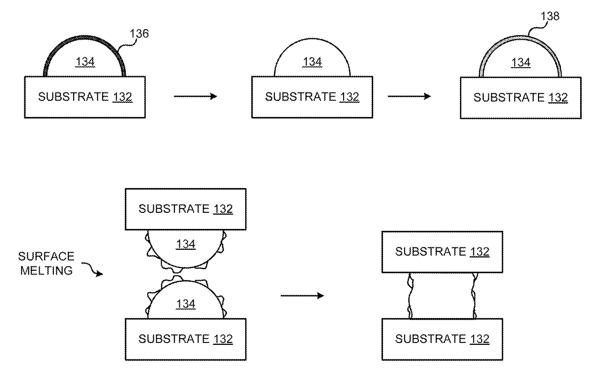
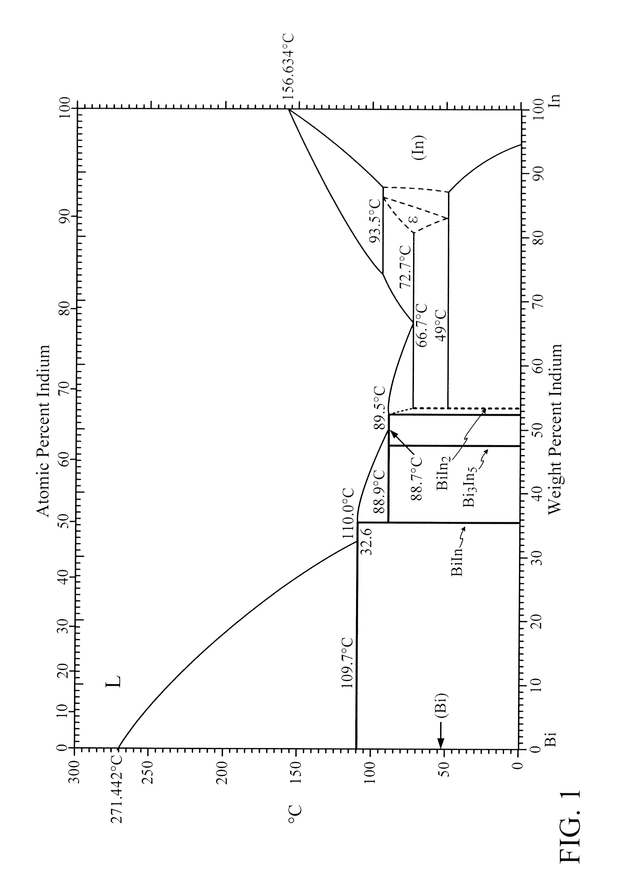
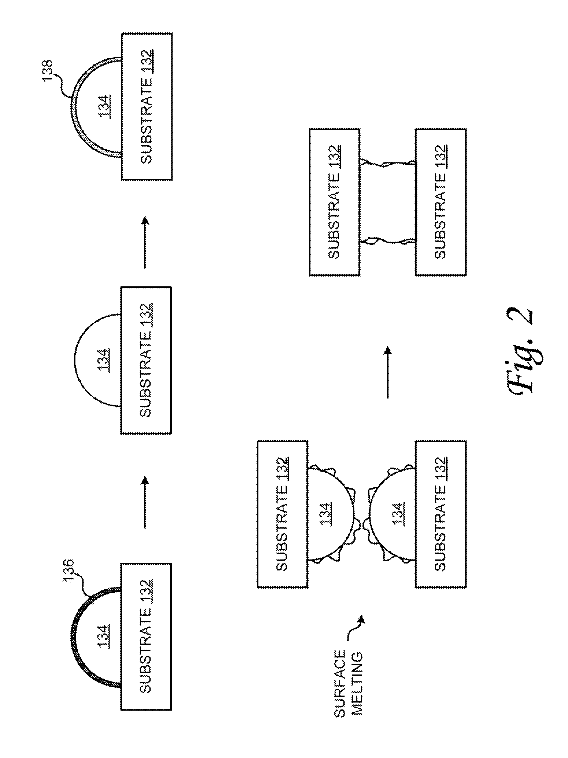
[0021]The present invention is directed toward compositions and structures, and toward methods for providing compositions and structures for metal bump bonding with relatively low temperatures, preferably lower than the melting temperature of indium. To obtain a lower processing temperature (preferred embodiments have a melting point of <100° C.), a metal coating method is provided using, in some embodiments, compositions of metals that have a eutectic reaction with indium with a relatively low eutectic temperature. For example, some compositions have a eutectic reaction with indium with a eutectic temperature lower than 150° C.

[0022]According to various embodiments, a metal or alloy layer is deposited on the indium bump surface. Preferably, the material is chosen such that the metal or alloy forms a passivation layer that is more resistant to oxidation than the underlying indium material. The passivation material is also preferably chosen to form a low melting temperature alloy wit...


PUM

PropertyMeasurementUnit
Fractionaaaaaaaaaa
Fractionaaaaaaaaaa
Fractionaaaaaaaaaa

Abstract

A process of making efficient metal bump bonding with relative low temperature, preferably lower than the melting point of Indium, is described. To obtaining a lower processing temperature (preferred embodiments have a melting point of <100° C.), a metal or alloy layer is deposited on the indium bump surface. Preferably, the material is chosen such that the metal or alloy forms a passivation layer that is more resistant to oxidation than the underlying indium material. The passivation material is also preferably chosen to form a low melting temperature alloy with indium at the indium bump surface. This is typically accomplished by diffusion of the passivation material into the indium to form a diffusion layer alloy. Various metals, including Ga, Bi, Sn, Pb and Cd, that can be used to form a binary to quaternary low melting point alloy with indium. In addition, diffusion of metal such as Sn, Sn—Zn into Ga—In alloy; Sn, Cd, Pb—Sn into Bi—In alloy; Cd, Zn, Pb, Pb—Cd into Sn—In alloy can help adjust the melting point of the alloy.

Description

CROSS-REFERENCE TO RELATED APPLICATIONS[0001]This application claims the benefit of U.S. Provisional Application No. 61 / 358,229, entitled Metal Coating for Improving Indium Bump Bonding, Filed on Jun. 24, 2010, which is herein incorporated by reference in its entirety.TECHNICAL FIELD[0002]The presently disclosed systems and methods relate generally to lead-free solders, and more particularly, some embodiments relate to systems, methods and technologies for allowing metal bump bonding with relatively low temperatures using a metal or alloy layer on the indium bump surface.DESCRIPTION OF THE RELATED ART[0003]Flip chip hybridization, sometimes known as bump bonding, is a process for microelectronics packaging and assembly that electrically and physically connects a chip to a substrate without the need for peripheral wirebonding. Conductive connections are provided using interconnect bumps made of a solder or indium material. This provides a low-profile connection with relatively low le...

Claims


Application Information

Patent Timeline
IPC IPC(8): H01B5/00B23K1/20B23K31/02
CPCH01L27/14636H01L24/81H01L2224/1357H01L2224/13582H01L2224/13583H01L2224/13599H01L2224/13605H01L2224/13609H01L2224/13611H01L2224/13613H01L2224/13616H01L2224/13618H01L2224/81193H01L2224/81201H01L2224/81801H01L2924/0103H01L2924/01047H01L2924/01049H01L2924/01078H01L2924/01082H01L2224/13109H01L24/16H01L24/13H01L24/11H01L27/14618H01L27/14634H01L2224/136H01L2224/1358H01L2924/014H01L2924/01322H01L2924/01075H01L2924/01033H01L2924/01006H01L2924/00013H01L2924/00014H01L2924/01083H01L2924/0102H01L2224/13099H01L2924/14H01L2924/15788H01L2924/00
Inventor CHEN, SIHAILEE, NING-CHENG
Owner INDIUM CORPORATION
Why Eureka
Try Eureka