Two-step flip chip bonding technique of focal-plane detector

A technology of focal plane detectors and process methods, which is applied in welding equipment, manufacturing tools, metal processing equipment, etc., can solve the problems of difficult process operation, difficult control of reverse welding offset, and easy formation of large blind elements, etc., to achieve improved The effect of flip soldering yield, improved connectivity, and convenient application

Active Publication Date: 2019-06-14
SHANGHAI INST OF TECHNICAL PHYSICS - CHINESE ACAD OF SCI
View PDF11 Cites 3 Cited by
  • Summary
  • Abstract
  • Description
  • Claims
  • Application Information

AI Technical Summary

Problems solved by technology

Thermocompression welding is a process in which the temperature of the photosensitive chip and the readout circuit is increased during the process of reverse welding, and then the two are interconnected by applying pressure, but the focal plane after high temperature alignment and interconnection drops to normal temperature due to Problems with thermal expansion mismatch between materials can make flip offset more difficult to control and are generally less used
Reflow soldering is to place the photosensitive chip and the readout circuit in a high temperature and reducing atmosphere (such as formic acid), remove the oxide layer on the surface of the indium column, cause the solder to reflow and form a physical connection between the photosensitive chip and the readout circuit, reflow soldering There is no need to apply pressure during the process, and the horizontal deviation after flip soldering is small, but the requirements for the flatness of the chip and the quality of the indium column in reflow soldering are much higher than those of cold pressure soldering, and the process operation is much more difficult, and it is easy to form Large blind elements, so the cold welding process is the most used at present
With the continuous expansion of the device scale and the continuous reduction of the pixel pitch, the indium column consistency and other problems introduced by the indium column preparation process have become increasingly prominent, and the random offset generated by the cold pressure welding process can easily exceed the limit range allowed by the effective interconnection , the reverse soldering process is increasingly becoming the bottleneck in the manufacturing process of large area array devices

Method used


Image

  • Two-step flip chip bonding technique of focal-plane detector
  • Two-step flip chip bonding technique of focal-plane detector

Examples


Embodiment

[0028] Embodiment: 1280×1024 element InGaAs focal plane flip welding process method

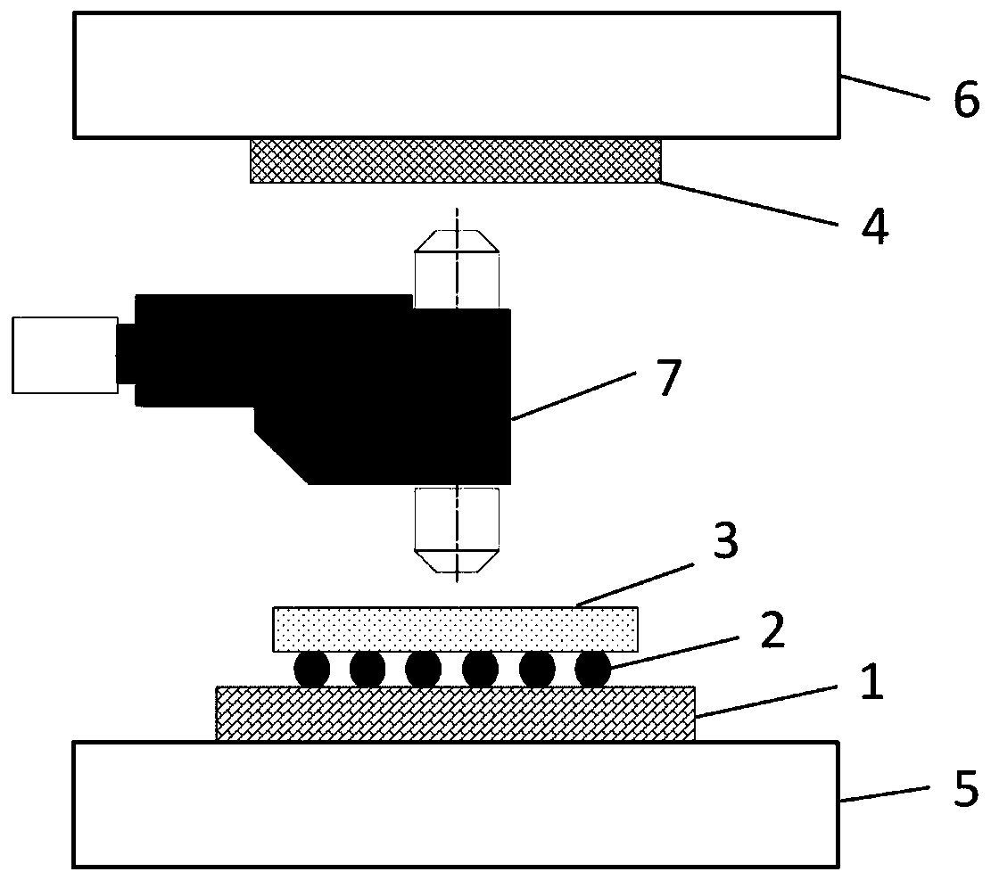
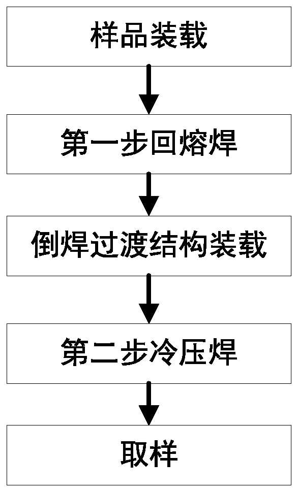
[0029] 1 Sample loading: prepare InGaAs photosensitive chip 3 and readout circuit 1 samples with double-sided growth of indium column 2, clean and clean them, place them in the corresponding trays, and operate the flip-bonding machine to vacuum the InGaAs photosensitive chip 3 and readout circuit 1 respectively. Adsorbed on the corresponding flip soldering fixture; the device size is 1280×1024 yuan, the center distance is 15μm, the photosensitive chip size is 20.0mm×16.2mm×0.35mm, and the readout circuit size is 22.0mm×20.0mm×0.48mm;

[0030] 2. The first step of remelting soldering: use the reverse soldering machine to align the microscope system 7 for leveling and alignment, and use the remelting soldering process to initially interconnect the InGaAs photosensitive chip 3 and the readout circuit 1 together, and inject formic acid during the remelting process Mixed gas with nitrogen, the tem...


PUM

PropertyMeasurementUnit
surface smoothnessaaaaaaaaaa

Abstract

The invention discloses a two-step flip chip bonding technique of a focal-plane detector. The two-step flip chip bonding technique of the focal-plane detector comprises the steps that a photosensitivechip and a reading circuit are interconnected preliminarily through a meltback welding technology; then a high-flatness material is adopted as a flip chip bonding transitional structure; and throughsecondary cold pressure welding of the flip chip bonding transitional structure and a preliminarily-interconnected focal-plane module, the photosensitive chip and the reading circuit are completely interconnected. According to the two-step flip chip bonding technique of the focal-plane detector, the meltback welding technology and the cold pressure welding technology are organically integrated; full play is given to advantages of the two technologies; flip chip bonding random shifting is reduced, and meanwhile, the problem of dis-interconnection caused by chip flatness and the indium bump quality is solved; thus the connectivity rate and the flip chip bonding finished product rate of a large-scale high-density focal-plane detector are effectively improved; and the technique is not limitedby array scales or pixel sizes and can be conveniently applied to various area array devices.

Description

technical field [0001] The invention belongs to the field of infrared and optoelectronics, and specifically relates to a two-step reverse welding process method of a focal plane detector, which is especially suitable for the preparation of large-scale high-density focal plane detectors. Background technique [0002] The focal plane detector needs to connect the discrete photosensitive chip and the components of the readout circuit one by one to form a focal plane device. The interconnection methods include direct flip-soldering hybrid, indirect flip-soldering hybrid, ring hole technology, and wire bonding. The direct reverse soldering hybrid infrared focal plane is the most mature focal plane structure at present. Its advantages are that the sensitive element array can obtain a duty factor close to 100%, the readout circuit can increase the area of ​​the signal processor, and the parasitic impedance is low. Strong anti-electromagnetic interference ability and high mechanical...

Claims


Application Information

Patent Timeline
Patent Type & Authority Applications(China)
IPC IPC(8): B23K28/02
Inventor 朱宪亮李雪黄松垒李淘邵秀梅张永刚龚海梅
Owner SHANGHAI INST OF TECHNICAL PHYSICS - CHINESE ACAD OF SCI
Why Eureka
Try Eureka