Indium features on multi-contact chips

a multi-contact chip and indium technology, applied in the direction of instruments, x/gamma/cosmic radiation measurement, radiation control devices, etc., can solve the problems of damage to the detector, physical and chemical fragility of the czt surface, and damage to the detector

Inactive Publication Date: 2004-10-07
CALIFORNIA INST OF TECH
View PDF1 Cites 3 Cited by
  • Summary
  • Abstract
  • Description
  • Claims
  • Application Information

AI Technical Summary

Benefits of technology

[0009] The CZT surface is physically and chemically delicate. The deposition of indium bumps using the wet photolithographic processes as described above inherently requires substantial handling of the chip and introduces possible chemical incompatibilities. Any type of chemical residue on the surface of the detector may increase leakage current.
[0024] FIG. 1 is a shadow mask used in an embodiment. The mask depicted has sixty-four circular apertures 2 disposed at predetermined positions corresponding to an 8.times.8 array of pixels found on a typical CZT detector. The mask is held above the surface of the detector or chip and indium is deposited through the apertures 2 onto the surface of the detector or chip. Larger-mechanical bumps are created during this deposition process by mechanical bump openings 4 supplied along the periphery of the 8.times.8 array of apertures 2. The optional mechanical bump openings 4 provide the resulting bump-bonded detector-readout device with greater mechanical stability. An alignment slot 6 is provided to align the mask with the detector or chip 14.

Problems solved by technology

One key issue is associated with the detailed steps leading to the electrical coupling of the detector to a corresponding readout chip.
These temperatures can be high enough to cause damage to the detector.
At temperatures above about 105.degree. C. damage begins to occur.
The CZT surface is physically and chemically delicate.
The deposition of indium bumps using the wet photolithographic processes as described above inherently requires substantial handling of the chip and introduces possible chemical incompatibilities.
Any type of chemical residue on the surface of the detector may increase leakage current.
A further drawback of the standard wet photolithographic technique is the problem of edge bead generation that occurs when the photoresist is spun onto a detector and the edges of the detector collect excess photoresist thereby causing a thicker region to form.
The lack of indium contacts at the edges may pose a problem when CZT detectors are arrayed together to form a larger area detector, as required in many applications.
In an array, a dead-space exists at each detector-detector interface, resulting in loss of effective overall detector area.
However, the trimming procedure introduces considerable risk to the detector at the end of the processing cycle through substrate contamination and breakage.
The resulting low yield of detectors may increase the cost of manufacture.
However, processes that require reflow of the solder bump produce wider bumps.
This can be disadvantageous not only do narrower electrical connections reduce electronic noise but they also allow more bumps to be formed over a smaller area, thus decreasing pitch advantageously.
Electronic noise is a significant limiting factor in the detector's ability to image radiation.
Higher bump heights may lower the capacitance and the lower the electronic noise.

Method used


Image

  • Indium features on multi-contact chips
  • Indium features on multi-contact chips
  • Indium features on multi-contact chips

Examples


example 2

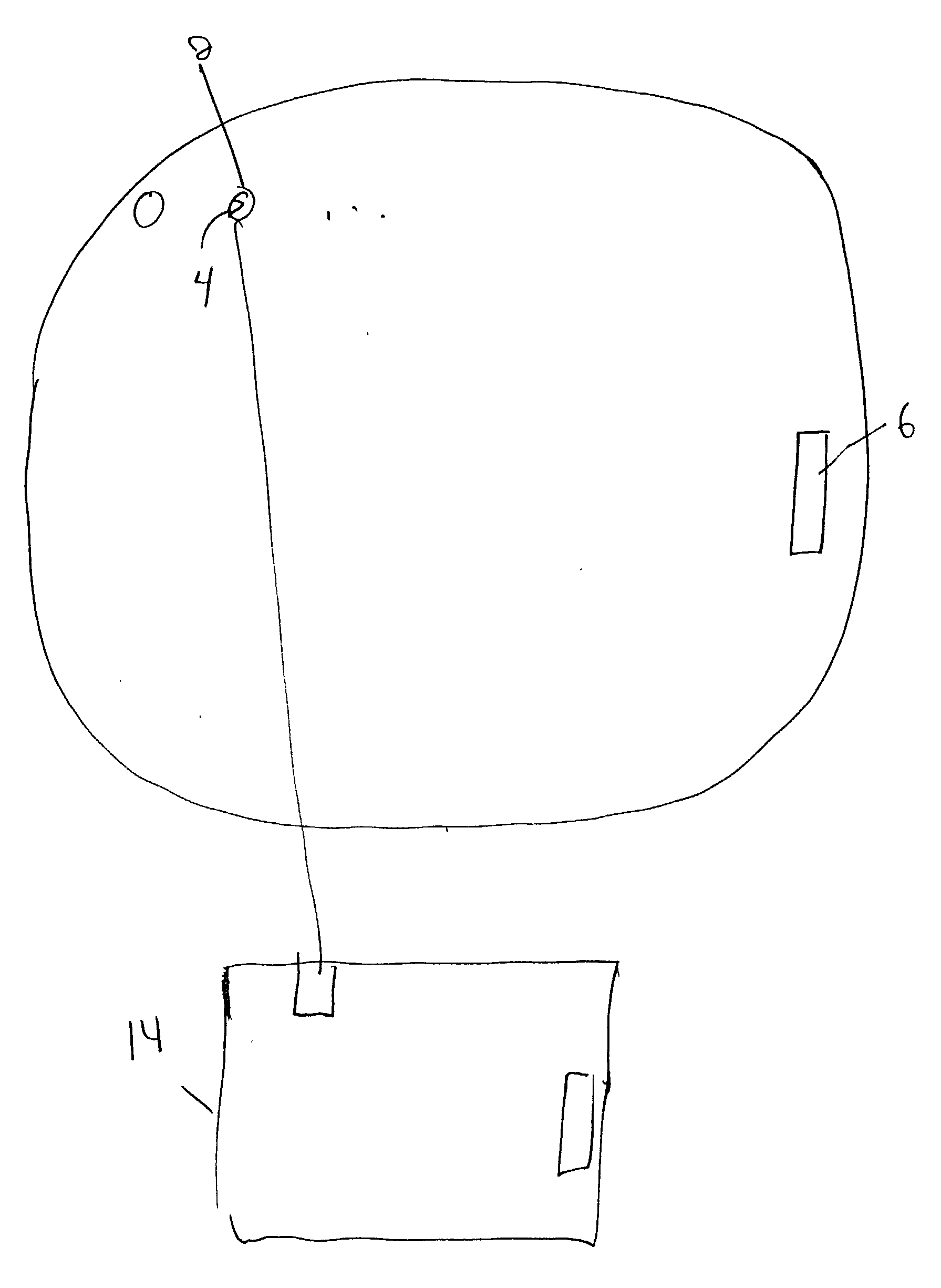
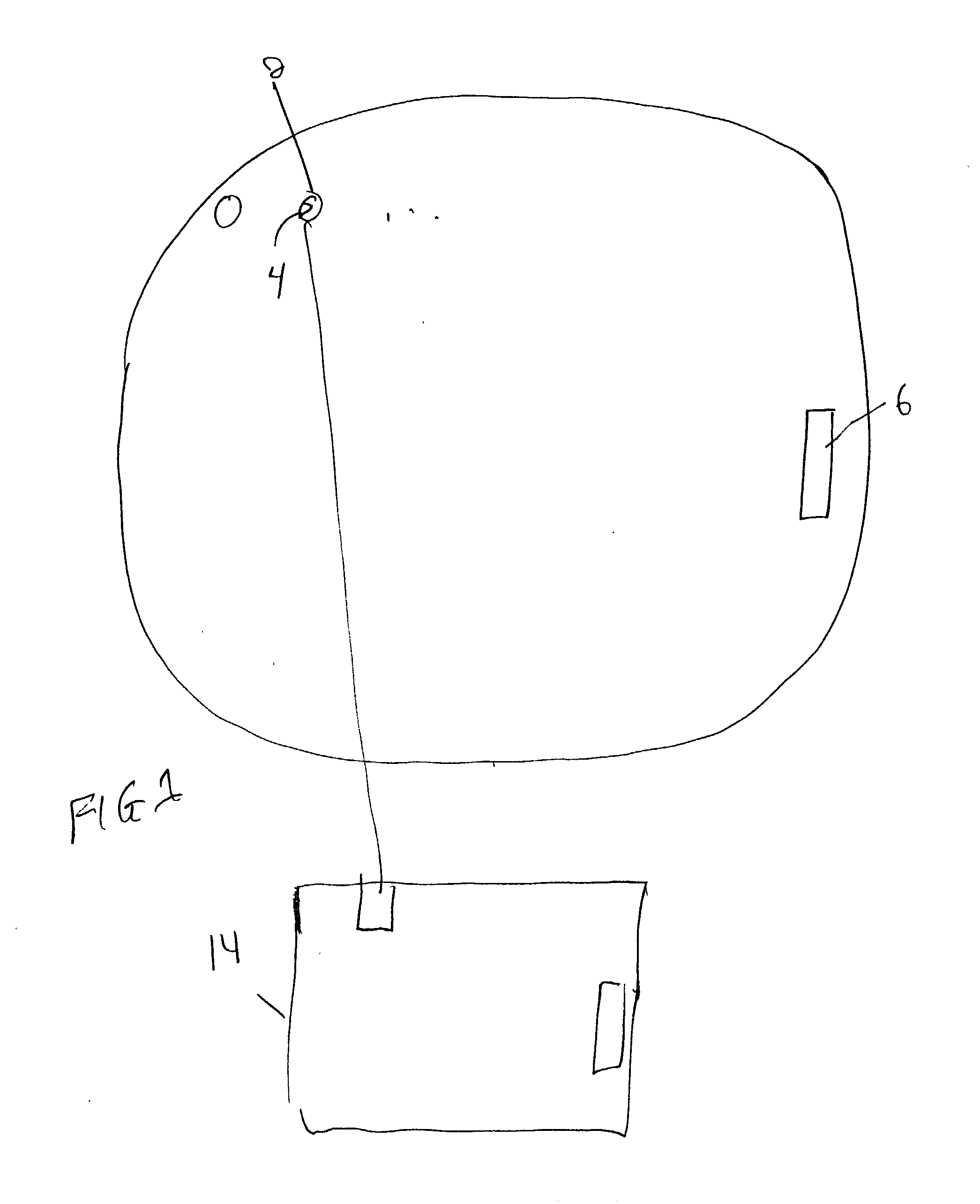
[0031] In another embodiment indium bumps are grown on a VLSI chip. The equipment and procedure are substantially the same as described in Example 1. A shadow mask is obtained with an array of holes matching the pixel pattern of the VLSI chip. The chip 14 and shadow mask 12 are constrained in the alignment fixture (FIG. 3), a precisely measured space is created between the mask and the chip with a Teflon spacer, the fixture is placed in a commercial mask aligner 26 (model Karl Suss MJB-3 IR), and the mask is precisely horizontally aligned above the VLSI chip. The alignment fixture is removed from the commercial mask aligner 26 and placed in an indium evaporation chamber and indium is deposited through the mask onto the chip's surface. As in Example 1, height of the bumps grown on the VLSI chip is determined by the size of the Teflon spacer used.

example 3

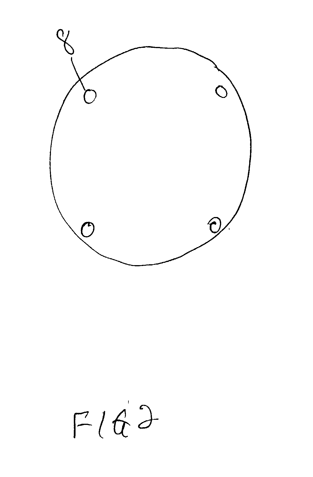
[0032] Using existing flip-chip technology, the CZT detector and the VLSI chip are bump bonded together to form a hybrid detector. A standard flip-chip alignment device is used for the process. A small (about 1 mm.times.1 mm) drop of a silicon adhesive is then placed on two or three of the corners of the resulting bump-bonded chip to provide additional mechanical strength. A silicon adhesive is used because it cures at room temperature, does not outgas contaminants and provides a joint that is resilient to shocks and vibrations. A silicon adhesive that is typically used is RTV 167 made by General Electric.


PUM


Abstract

A device comprising a pixilated semiconductor detector or VLSI chip having plurality of individual indium bumps arrayed on a surface of the detector, wherein the indium bumps are in electrical contact with the surface and are situated in defined locations on the surface is provided. Additionally, a hybrid detector comprising a pixilated detector in electrical contact with a VLSI chip, wherein electrical contacts formed from indium metal are made between the pixels of the semiconductor and regions on the VLSI chip corresponding thereto is provided. In another embodiment, a method of forming electrical contacts on a pixilated detector comprising the steps of constraining a shadow mask having an array of holes in predetermined locations above a surface on the detector, aligning the mask above the detector, and evaporating indium metal under vacuum through holes in the mask onto the surface of the detector to form the contacts is described.

Description

[0001] The present application claims benefit of U.S. Provisional Application No. 60 / 184,502, filed Feb. 23, 2000.[0003] The present invention relates to semiconductor detectors and chips for use in imaging devices and also to methods for forming indium features on a surface of such a detector or chip.BACKGROUND AND SUMMARY[0004] Pixilated multi-contact detectors employing semiconductors, such as Si, Ge, HgI, CdTe, and CdZnTe, with readout chips are currently under development in many research laboratories. These detectors are key components in imaging systems with medical, industrial, and scientific applications. For example, the CdZnTe (CZT) semiconductor detector is a device for the imaging and spectroscopy of hard X-rays and low-energy gamma-rays. The CZT detector demonstrates improved room temperature spatial and energy resolution of X-rays. CZT multi-contact detectors are being developed, in one instance, for use in medical scanners and homographs. Typically, each imagining sy...

Claims


Application Information

Patent Timeline
Patent Type & Authority Applications(United States)
IPC IPC(8): G01T1/24H01L21/60H01L27/146H01L31/0296
CPCH01L24/11H01L27/14601H01L27/14634H01L27/14661H01L27/14683H01L27/14696H01L31/0224H01L31/02966H01L31/0324H01L31/18H01L2224/13099H01L2924/01027H01L2924/0103H01L2924/01039H01L2924/01049H01L2924/01052H01L2924/01077H01L2924/01082H01L2924/01322H01L2924/30105H01L2924/01006H01L2924/01033H01L2924/014H01L2924/00014H01L2924/12042H01L2924/00H01L2224/0401
Inventor MATTHEWS, BRIANSCHINDLER, STEPHEN M.BOLOTNIKOV, ALEKSEY E.
Owner CALIFORNIA INST OF TECH
Why Eureka
Try Eureka