Quanta trap infrared detector for multi-folded light dispersion coupling

A technology of infrared detectors and multi-quantum well layers, which is applied in the direction of electric solid-state devices, semiconductor devices, semiconductor/solid-state device components, etc., can solve the problems that quantum well devices cannot be detected, and achieve low process difficulty and high coupling efficiency Effect

Inactive Publication Date: 2008-05-28
SHANGHAI INST OF TECHNICAL PHYSICS - CHINESE ACAD OF SCI
View PDF0 Cites 3 Cited by
  • Summary
  • Abstract
  • Description
  • Claims
  • Application Information

AI Technical Summary

Problems solved by technology

It is also clearly seen that the inability of quantum well devices to detect under normal incidence conditions has constituted one of the main shortcomings of this type of detector. Although the preparation of gratings can solve this shortcoming in principle, this is by sacrificing The simplicity of the process is achieved by

Method used


Image

  • Quanta trap infrared detector for multi-folded light dispersion coupling
  • Quanta trap infrared detector for multi-folded light dispersion coupling

Examples


Embodiment Construction

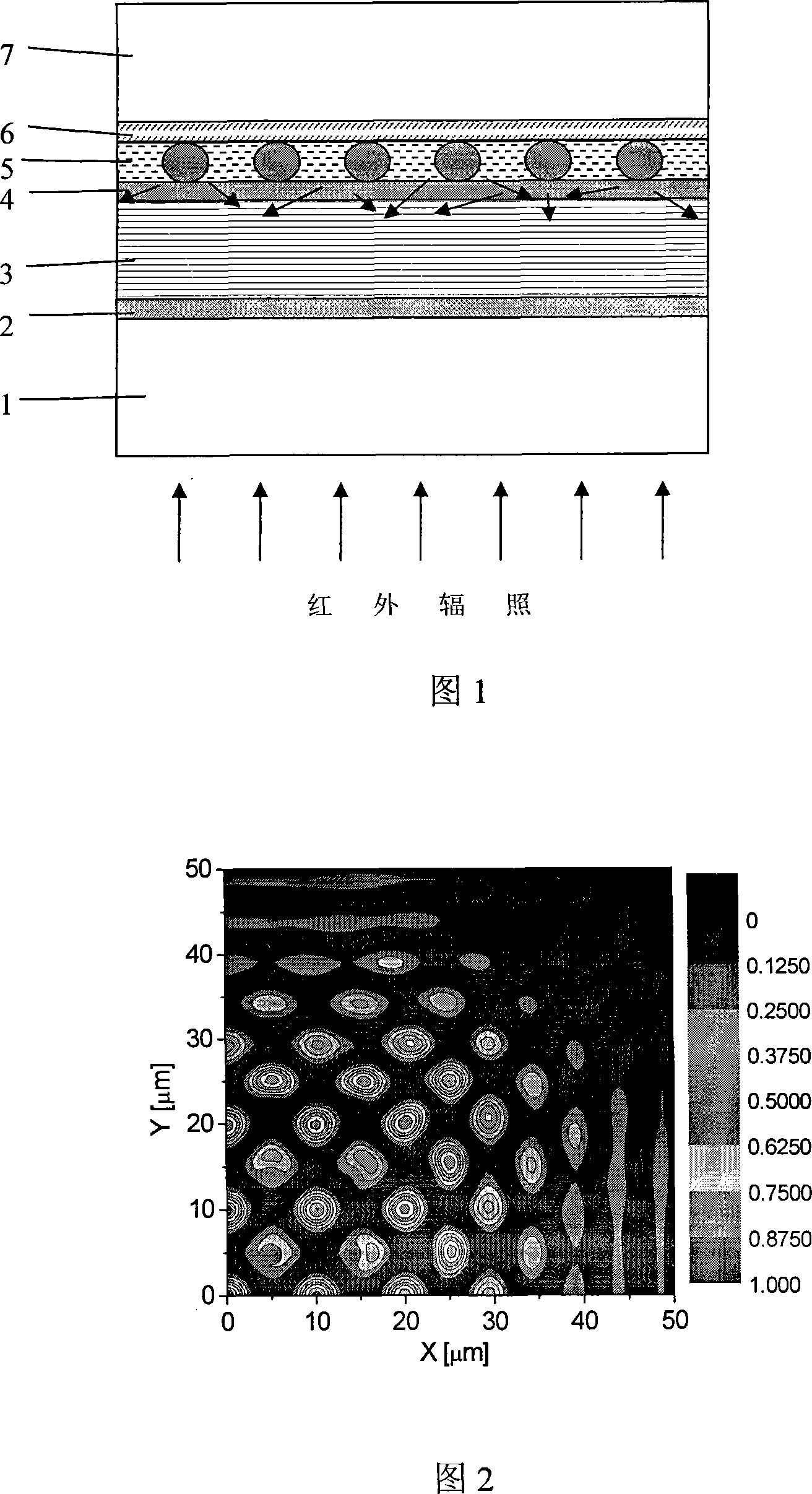
[0016] Below is GaAs / Al with a peak detection wavelength of 9.5 μm x Ga 1-x Taking As quantum well infrared detector as an example, the specific implementation of the present invention will be further described in detail in conjunction with the accompanying drawings.

[0017] See Fig. 1, the quantum well infrared detector involved in the present invention comprises: GaAs substrate layer 1, on GaAs substrate layer 1 by molecular beam epitaxy or metal-organic chemical vapor deposition successively layer-by-layer growth:

[0018] n-type doped GaAs lower electrode layer 2 with a doping concentration of 1.0×10 18 cm -3 ;

[0019] 50-period multi-quantum well layer 3;

[0020] n-type doped GaAs upper electrode layer 4;

[0021] On the GaAs upper electrode layer 4 is distributed an array layer 5 formed of metal balls submerged in an organic adhesive that is firmly in contact with the upper electrode layer 4 . The area of ​​the covered metal ball layer should be the area of ​​th...


PUM


Abstract

The invention discloses a quantum well infrared detector of multiple light scattering coupling. The detector comprises a substrate layer, a lower electrode layer which grows successively layer by layer, a multiple quantum well layer with 50 periods and an upper electrode layer. An array layer made of metallic balls which are immersed in organic adhesive or balls which are coated with metal is provided on the upper electrode layer. The array layer is provided with a metal contacting layer, and the metal contacting layer is provided with a readout circuit by means of flip-chip bonding interconnection to realize the readout detection signals. The invention has the advantages that: firstly, the metal ball array replaces the traditional grating. The electric rector which can be absorbed with transition by a quantum well belt is produced by multiple light coupling among the metallic balls. The electric rector parallels to the component of the quantum well layer, so the coupling between the normal incidence lights and the quantum well is realized. Secondly, the metallic ball array replaces the traditional indium column of flip-chip bonding interconnection to form an anisotropic conducting layer, so the conductive function is realized. Because of the advantages, on one hand, the coupling efficiency of normal incidence lights is improved; on the other hand, the deposition of indium bump is saved, and the flip-chip bonding process is simplified.

Description

technical field [0001] The invention relates to a quantum well infrared detector, in particular to an n-type semiconductor quantum well infrared detector. Background technique [0002] Among the current quantum well infrared detectors, the closest to commercial production is n-type GaAs / AlGaAs multi-quantum well infrared focal plane devices, which have been commercially developed by companies such as France and the United States, and their scale has reached 256×256 or even 512×512, for this reason, the size of the photosensitive element on the focal plane has also reached 30 microns or even smaller in linear dimension. However, since in principle this type of infrared detector does not respond to normal incident infrared radiation, one must adopt the basic structure of grating coupling on the focal plane device. The specific structural parameters of the grating are sensitive to the coupling efficiency of infrared radiation, so the grating must be finely prepared, which undo...

Claims


Application Information

Patent Timeline
Patent Type & Authority Applications(China)
IPC IPC(8): H01L25/16H01L23/488
Inventor 李志锋陆卫熊大元陈效双李宁甄红楼张波陈平平李天信
Owner SHANGHAI INST OF TECHNICAL PHYSICS - CHINESE ACAD OF SCI
Why Eureka
Try Eureka