Method and apparatus for recovering pattern on silicon substrate

a technology of silicon substrate and pattern, which is applied in the direction of cleaning process and apparatus, lighting and heating apparatus, cleaning using liquids, etc., can solve the problems of pattern collapse, pattern collapse, and the space between the patterns is filled with foreign substances or the pattern is not suitable for wet etching

Inactive Publication Date: 2011-07-21
TOKYO ELECTRON LTD
View PDF13 Cites 3 Cited by
  • Summary
  • Abstract
  • Description
  • Claims
  • Application Information

AI Technical Summary

Benefits of technology

[0011]In view of the above, the present invention provides a method and an apparatus capable of recovering a shape of patterns, formed on a silicon substrate by etching, by removing foreign substance grown between the patterns.

Problems solved by technology

However, the formation of the ultra-fine patterns causes the following problems.
Further, if the silicon substrate is left in the air for a long period of time, the foreign substance grown between the patterns may cause collapse of the patterns.
Further, it is believed that the phenomenon in which the spaces between the patterns are filled with the foreign substances or the patterns collapse due to the fine widths of the patterns and the spaces between the patterns.
Hence, in case of the fine patterns having about 32 nm line width and space, it is not proper to perform the wet etching.
As described above, in case the fine patterns having the line width and space of about 32 nm or less are formed on a silicon substrate, the spaces between the patterns may be filled with the foreign substance, or the foreign substances may cause collapse of the patterns.
Further, in this case, it is not proper to perform the wet etching process.

Method used


Image

  • Method and apparatus for recovering pattern on silicon substrate
  • Method and apparatus for recovering pattern on silicon substrate
  • Method and apparatus for recovering pattern on silicon substrate

Examples


Embodiment Construction

[0018]An embodiment of the present invention will be described with reference to the accompanying drawings which form a part hereof.

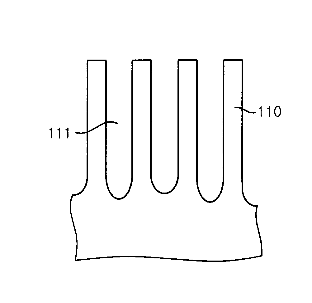
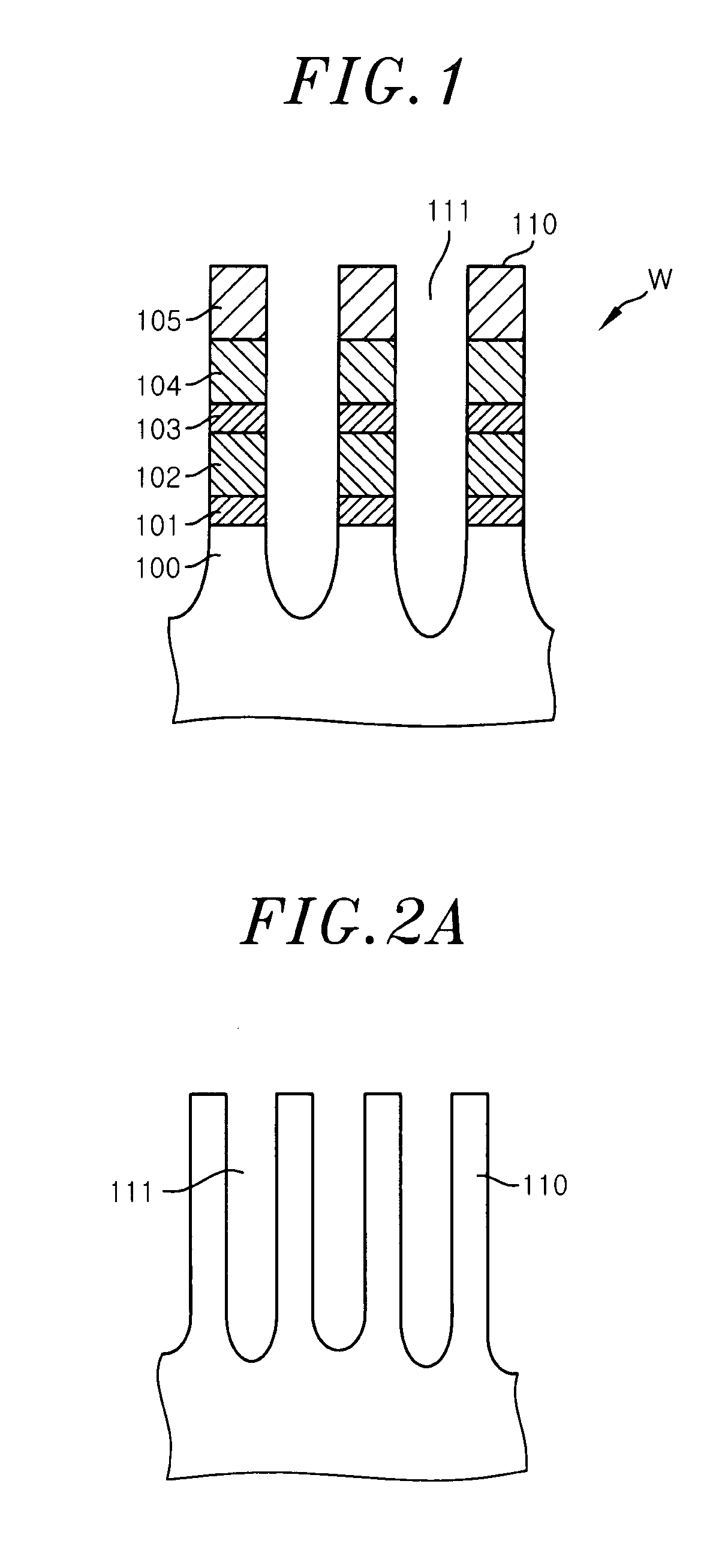
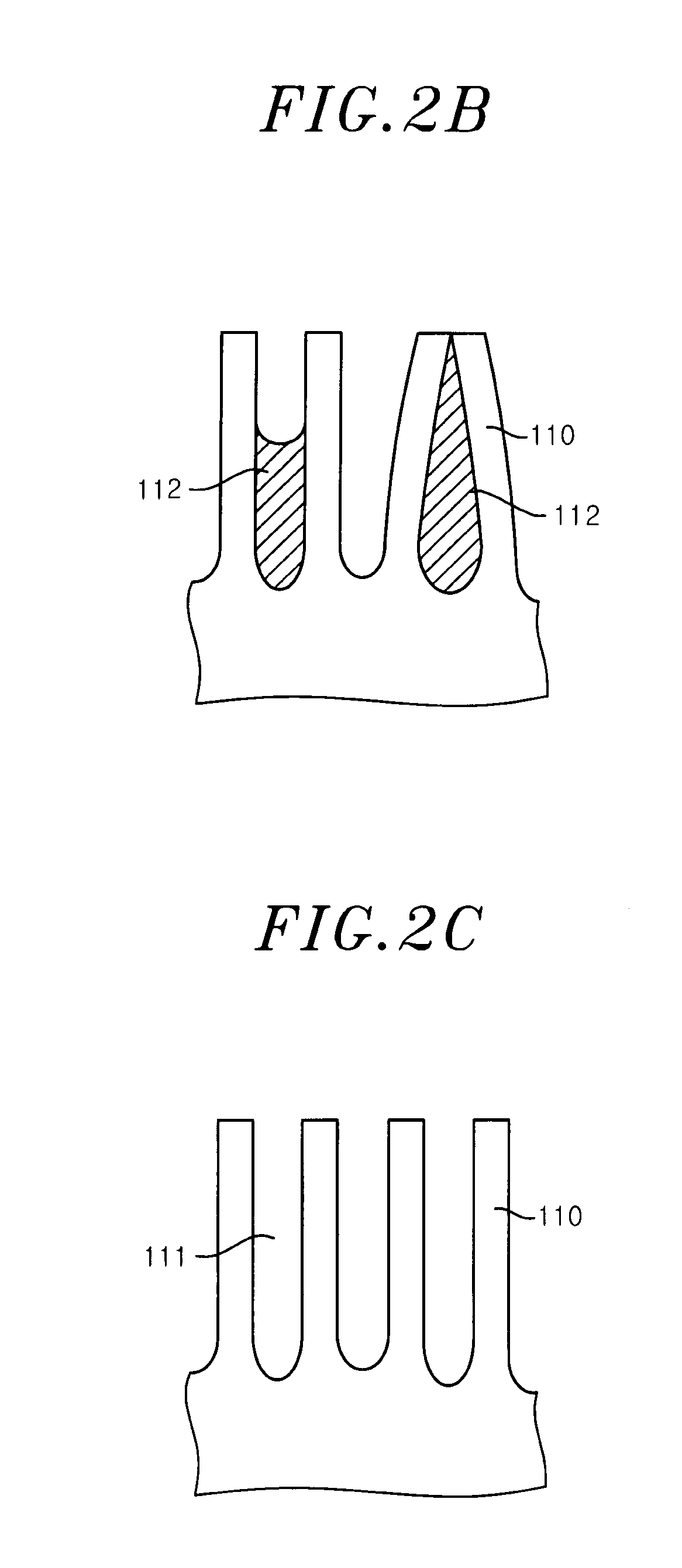
[0019]FIG. 1 schematically shows an example of patterns to be recovered by a method and an apparatus for recovering patterns on a silicon substrate in accordance with the embodiment of the present invention. As shown in FIG. 1, patterns 110, which are formed of lines spaced apart from each other at regular intervals, are formed on a silicon substrate (semiconductor wafer) W by etching. Further, spaces 111 are formed between the patterns 110. In the present embodiment, the widths of the patterns 110 and the spaces 111 are not greater than about 32 nm.

[0020]Each of the patterns 110 on a silicon substrate W includes, e.g., a single crystal silicon layer 100, an SiO2 layer 101, a polysilicon layer 102, an SiO2 layer 103, an SiN layer 104, an SiO2 layer 105 and the like which are laminated in that order from the bottom.

[0021]Hereinafter, a method for recover...


PUM

PropertyMeasurementUnit
temperatureaaaaaaaaaa

Abstract

A method for recovering a shape of patterns, formed etching on a silicon substrate by etching, by removing foreign substances grown between the patterns is provided. The method includes heating the silicon substrate accommodated in a chamber to a temperature of about 160° C. or higher.

Description

CROSS-REFERENCE TO RELATED APPLICATIONS[0001]This application claims priority to Japanese Patent Application No. 2010-009979 filed on Jan. 20, 2010, and U.S. Provisional Application No. 61 / 306,097 filed on Feb. 19, 2010 the entire contents of which are incorporated herein by reference.FIELD OF THE INVENTION[0002]The present invention relates to a method and an apparatus for recovering patterns on a silicon substrate.BACKGROUND OF THE INVENTION[0003]In a semiconductor device manufacturing process, fine circuit patterns are formed on a silicon substrate (semiconductor wafer) by a photolithography process. In the photolithography process, predetermined patterns, e.g., lines, holes or the like, are formed on a silicon substrate by a process for coating, exposing and developing a photoresist, an etching process using the photoresist as a mask, and the like.[0004]When the etching is performed in the photolithography process, a polymer (so-called sidewall polymer) may be adhered to sidewal...

Claims


Application Information

Patent Timeline
Patent Type & Authority Applications(United States)
IPC IPC(8): B08B7/00
CPCH01L21/02057H01L21/02041H01L21/02049H01L21/324H01L21/67028
Inventor NISHIMURA, EIICHITAHARA, SHIGERUYAMASHITA, FUMIKO
Owner TOKYO ELECTRON LTD
Why Eureka
Try Eureka