Package structure having MEMS element

a technology of packaging structure and element, applied in the direction of transducer details, semiconductor devices, semiconductor/solid-state device details, etc., can solve the problems of increasing high cost of lid b>12/b> by drilling, and inability to meet the demand for miniaturization. , to achieve the effect of reducing the thickness of the overall structur

Active Publication Date: 2011-07-21
SILICONWARE PRECISION IND CO LTD
View PDF9 Cites 27 Cited by
  • Summary
  • Abstract
  • Description
  • Claims
  • Application Information

AI Technical Summary

Benefits of technology

[0018]According to the present invention, the package structure having at least a Micro Electro Mechanical System (MEMS) element is provided directly on a wafer without the need of a carrier, thus reducing the thickness of the overall structure. Further, the position of the bumps is not limited to the top of the lid. Instead, the bumps are disposed at any positions of the top surface of the package structure. Furthermore, the lid is connected to a ground end through the sub-bonding wires and the metallic traces so as to achieve an EMI shielding effect.

Problems solved by technology

However, the use of the carriers (the substrate 10 of FIG. 1A and the lead frame 10′ of FIG. 1B) increases the thickness of the overall structures and cannot meet the demand for miniaturization.
However, forming the conductive through holes 120 in the lid 12 by drilling incurs high costs.
In addition, misalignment or unstable connection can easily occur to the contact pads 122 which flank the conductive through holes 120, thus leading to poor electrical connection and further adversely affecting the electrical connection quality between the chip 14 and the external electronic element.
However, the above package structure requires a lithography process for forming the traces on the lid, thus incurring high costs.
In addition, the solder balls 16 are confined to the vicinity of the lid to thereby cause solder ball bridge, limit the signal input / output density of the package structure and reduction of the trace spacing, add to the difficulty in attaching the package structure to a circuit board.
As such, the application field of the package structure is limited.
In addition, corresponding to the package structure, a fine pitch circuit board is required, thus increasing the cost.
Further, such a package structure cannot achieve an EMI shielding effect.

Method used


Image

  • Package structure having MEMS element
  • Package structure having MEMS element
  • Package structure having MEMS element

Examples


first embodiment

[0027]FIGS. 2A to 2F are cross-sectional views showing a package structure having at least a Micro Electro Mechanical System (MEMS) element according to a first embodiment of the present invention.

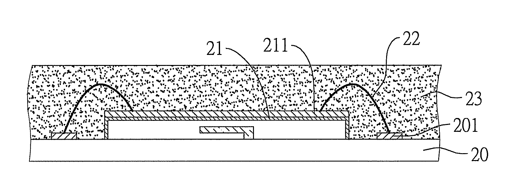
[0028]Referring to FIG. 2A, a wafer 20 is prepared, which has a plurality of electrical connection pads 201 and a plurality of MEMS elements 202. It should be noted that only a portion of the wafer is shown in FIG. 2A.

[0029]Referring to FIG. 2B, a plurality of lids 21 is disposed on the wafer 20 for covering the MEMS elements 202, respectively. The wafer 20 is made of silicon. The MEMS elements 202 are gyroscopes, accelerometers or RF MEMS elements. The lids 21 are made of a conductive material or a non-conductive material such as glass, silicon, metal or ceramic. A metal layer 211 or a plurality of bonding pads, as shown in FIG. 2B′, is further provided on each of the lids 21 by such as sputtering, which are made of Al, Cu, Au, Pd, Ni / Au, Ni / Pd, TiW / Au, Ti / Al, TiW / Al, Ti / Cu / Ni / Au or a com...

second embodiment

[0045]FIG. 3 is a cross-sectional view of a package structure 3 having a MEMS element according to a second embodiment of the present invention. The package structure 3 of FIG. 3 is similar to the package structure 2 of FIG. 2F, but the main difference therebetween is that the metal layer 211 of the package structure 3 is composed of a plurality of bonding pads, and the metallic traces 24 electrically connect to the first sub-bonding wires 221 and the second sub-bonding wires 222, respectively.

third embodiment

[0046]FIG. 4 is a cross-sectional view of a package structure 4 having a MEMS element according to a third embodiment of the present invention. The package structure 4 in the third embodiment is similar to the package structure 2 of FIG. 2F, but a main difference therebetween is that the top surface of the encapsulant 23 of the package structure 4 is flush with the top surface of the lid 21, i.e., the metal layer 211 is exposed from the encapsulant 23, and the second sub-bonding wires 222 are removed at the time a portion of the encapsulant 23 is removed. As such, the first sub-bonding wires 221 are remained for electrically connecting to the electrical connection pads 201, and the top ends of the first sub-bonding wires 221 are exposed from the top surface of the encapsulant 23.


PUM


Abstract

A package structure having at least an MEMS element is provided, including a chip having electrical connecting pads and the MEMS element; a lid disposed on the chip to cover the MEMS element and having a metal layer provided thereon; first sub-bonding wires electrically connecting to the electrical connecting pads; second sub-bonding wires electrically connecting to the metal layer; an encapsulant disposed on the chip, wherein the top ends of the first and second sub-bonding wires are exposed from the encapsulant; and metallic traces disposed on the encapsulant and electrically connecting to the first sub-bonding wires. The package structure advantageously features reduced size, relatively low costs, diverse bump locations, and an enhanced EMI shielding effect.

Description

BACKGROUND OF THE INVENTION[0001]1. Field of the Invention[0002]The present invention relates to package structures, and more particularly, to a package structure having at least a Micro Electro Mechanical System (MEMS) element.[0003]2. Description of Related Art[0004]Micro Electro Mechanical System (MEMS) techniques integrate electrical and mechanical functions into a single element using microfabrication technology. A MEMS element is disposed on a chip and covered by a shield or packaged with an underfill adhesive so as to form a MEMS package structure. FIGS. 1A to 1F are cross-sectional views showing different package structures with a MEMS element.[0005]FIG. 1A shows a package structure disclosed by U.S. Pat. No. 6,809,412. Referring to FIG. 1A, the package structure comprises a substrate 10, a chip 14 disposed on the substrate 10 and having a MEMS element 141, a plurality of bonding wires 11 electrically connecting the substrate 10 and the chip 14, and a lid 12 disposed on the ...

Claims


Application Information

Patent Timeline
Patent Type & Authority Applications(United States)
IPC IPC(8): H01L29/84H01L23/52
CPCB81B7/007H01L21/56H01L23/315H01L23/552H01L2224/48227H01L2224/48465H01L2924/01013H01L2924/01029H01L2924/01046H01L2924/01079H01L2924/09701H01L2924/3025H01L2924/1461B81B2207/095H01L24/48H01L2924/00H01L2924/12042H01L2924/181H01L2924/00014H01L2924/00012H01L2224/45099H01L2224/45015H01L2924/207B81B7/0064
Inventor CHIU, CHI-HSINHUANG, CHIH-MINGCHAN, CHANG-YUEHLIAO, HSIN-YIKE, CHUN-CHI
Owner SILICONWARE PRECISION IND CO LTD
Why Eureka
Try Eureka